


Researchers from Xiamen University of Technology have published a dissertation titled "Defect modulation and enhanced p-type conductivity in Mg-N co-doped Ga₂O₃ thin films grown by pulsed laser deposition" in Journal of Alloys and Compounds.
Background
Ultra-wide-bandgap Ga₂O₃ semiconductors show great application prospects in power electronics and solar-blind optoelectronic devices. However, constrained by deep acceptor levels and donor self-compensation originating from oxygen vacancies, the realization of stable p-type Ga₂O₃ remains a critical challenge, which severely limits the development of bipolar devices and complementary oxide electronics. Previous researches have explored p-type conduction via single Mg or N doping. Nevertheless, single-dopant approaches usually suffer from low acceptor activation efficiency and cannot effectively suppress the compensation effect from oxygen-vacancy defects, leading to limited improvement in hole concentration and device performance. Although co-doping defect-engineering strategies have been proposed theoretically, the modulation effect of Mg-N co-doping on defect states and electronic structures in amorphous Ga₂O₃ films is not fully understood. The correlation among defect suppression, Fermi-level modulation and electrical-device performance has not been systematically clarified. There is a lack of feasible low-temperature routes for fabricating high-performance p-type Ga₂O₃ films, which hinders the further development of Ga₂O₃-based bipolar optoelectronic devices.
Abstract
Achieving stable p-type conductivity in Ga₂O₃ remains a major challenge because acceptor activation is strongly limited by deep acceptor levels and oxygen-vacancy donor self-compensation. In this work, Mg-N co-doped amorphous Ga₂O₃ thin films were deposited by pulsed laser deposition to investigate the role of co-doping in oxygen-vacancy defect modulation and p-type activation. Compared with single Mg or N doping, Mg-N co-doping significantly suppressed oxygen-vacancy defects to 4.83%, and decreased the energy separation between Fermi level and valence band maximum to 1.57 eV, which indicates that Mg-N co-doping facilitates p-type conduction with higher hole activation concentration in Ga₂O₃ film. Hall-effect measurements revealed enhanced hole-dominated transport mechanism in the Mg-N co-doped films, with the hole concentration increased to 5.2 × 10¹⁵ cm⁻³, indicating improved acceptor activation efficiency. Furthermore, Ga₂O₃ homojunction diodes fabricated using the Mg-N co-doped film showed the highest rectification ratio of 4.27 × 10³, the lowest ideality factor of 2.05, and the lowest turn-on voltage of 8.38 V among the investigated devices. The improved electrical and device properties are due to the synergistic effects of oxygen-vacancy suppression and band-structure modulation induced by Mg-N co-doping. This work demonstrates an effective defect-engineering strategy for improving p-type conduction mechanism in amorphous Ga₂O₃ thin films and provides insight into the development of Ga₂O₃-based bipolar oxide devices.
Highlights
A low-temperature and cost-effective approach for realizing p-type Ga₂O₃films has been proposed using PLD at RT via Mg-N co-doped technique.
Compared with single Mg or N doping, Mg-N co-doping significantly suppresses oxygen-vacancy defects relieving donor self-compensation in Ga₂O₃film.
Mg-N co-doping introduces acceptor states and makes the Fermi level closer to the valence band maximum, which facilitates p-type conduction with higher hole activation concentration in Ga₂O₃film.
Ga₂O₃p-n homojunction diodes were fabricated and exhibited superior rectification characteristics.
Conclusion
In this study, undoped, N-doped, Mg-doped, and Mg-N co-doped amorphous Ga₂O₃ thin films were deposited at RT by PLD. All films exhibited high optical transparency and predominantly amorphous characteristics. Compared with single N or Mg doping, Mg-N co-doping more effectively modulated the oxygen-vacancy defect and electronic structure of amorphous Ga₂O₃ films. XPS analysis revealed that Mg-N co-doping significantly suppressed oxygen-vacancy defects, reducing the OV ratio to 4.83%. UPS results further showed that the energy separation between the Fermi level and the VBM is low to 1.57 eV indicating easier hole activation and conduction. Hall-effect measurements demonstrated enhanced hole-dominated transport behavior in the Mg-N co-doped films with a higher hole concentration of 5.2 × 10¹⁵ cm⁻³. Moreover, Ga₂O₃ homojunction diodes fabricated using the Mg-N co-doped film showed the best rectifying performance among the investigated devices, including the highest rectification ratio of 4.27 × 10³, the lowest ideality factor of 2.05, and the lowest turn-on voltage of 8.38 V. These results confirm that Mg–N co-doping can simultaneously suppress donor-like defects, modulate the band structure of Ga₂O₃ film, enhance junction transport characteristics. Although the device performance is still limited by the relatively low mobility and large transport resistance of the amorphous films, the present results demonstrate that Mg-N co-doping is an effective strategy for improving p-type conduction behavior and rectifying homojunction characteristics in amorphous Ga₂O₃ thin films. Compared with previously reported p-type Ga₂O₃ films and homojunctions, this work provides a low-thermal-budget approach for oxygen-vacancy defect modulation and electronic-structure engineering in Ga₂O₃, which may provide useful guidance for the development of Ga₂O₃-based bipolar oxide devices, transparent oxide electronics, and thermally sensitive semiconductor device applications.
Project Support
This work is sponsored by Natural Science Foundation of Fujian Province (No. 2023J011459, No. 2024J011213, No. 2020H0025), Natural Science Foundation of Xiamen (No. 3502Z202373061), National Natural Science Foundation of China (No. 61904155), Science and technology Project of Fujian Provincial Department of Education (No. JAT200484). This study is also sponsored by Fujian Association for Science and Technology.
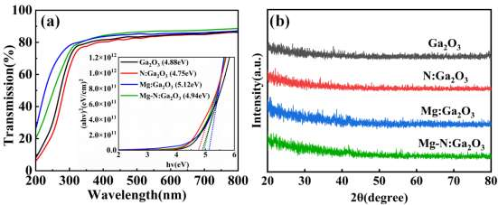
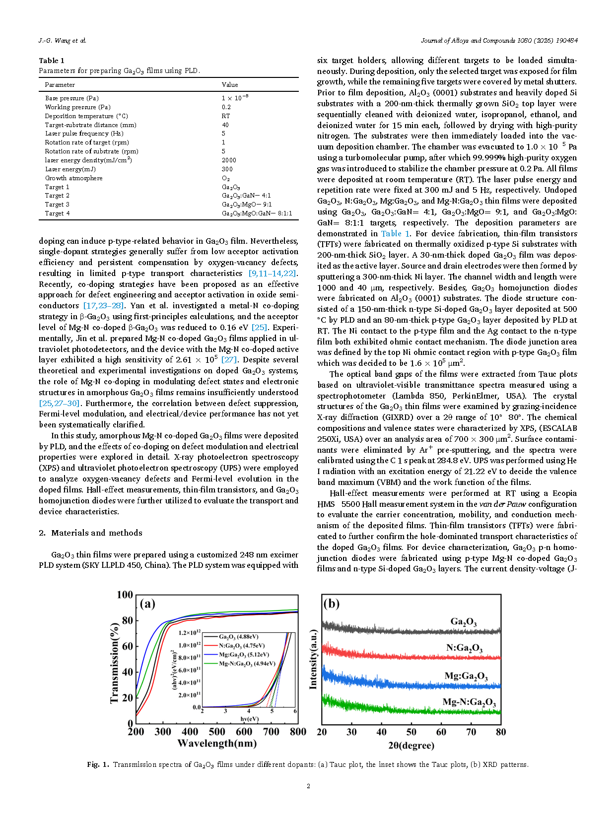
Fig. 1 Transmission spectra of Ga₂O₃ films under different dopants: (a) Tauc plot, the inset shows the Tauc plots, (b) XRD patterns.
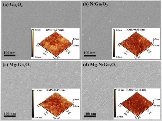
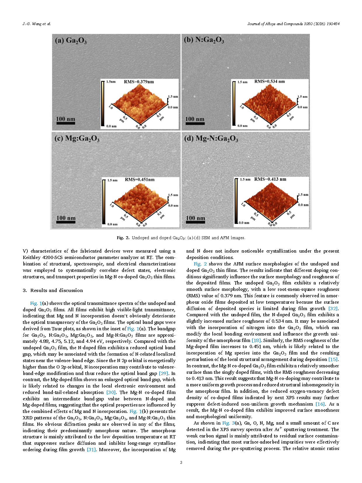
Fig. 2 Undoped and doped Ga₂O₃ : (a)-(d) SEM and AFM images.
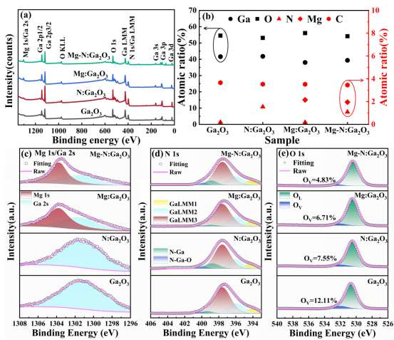
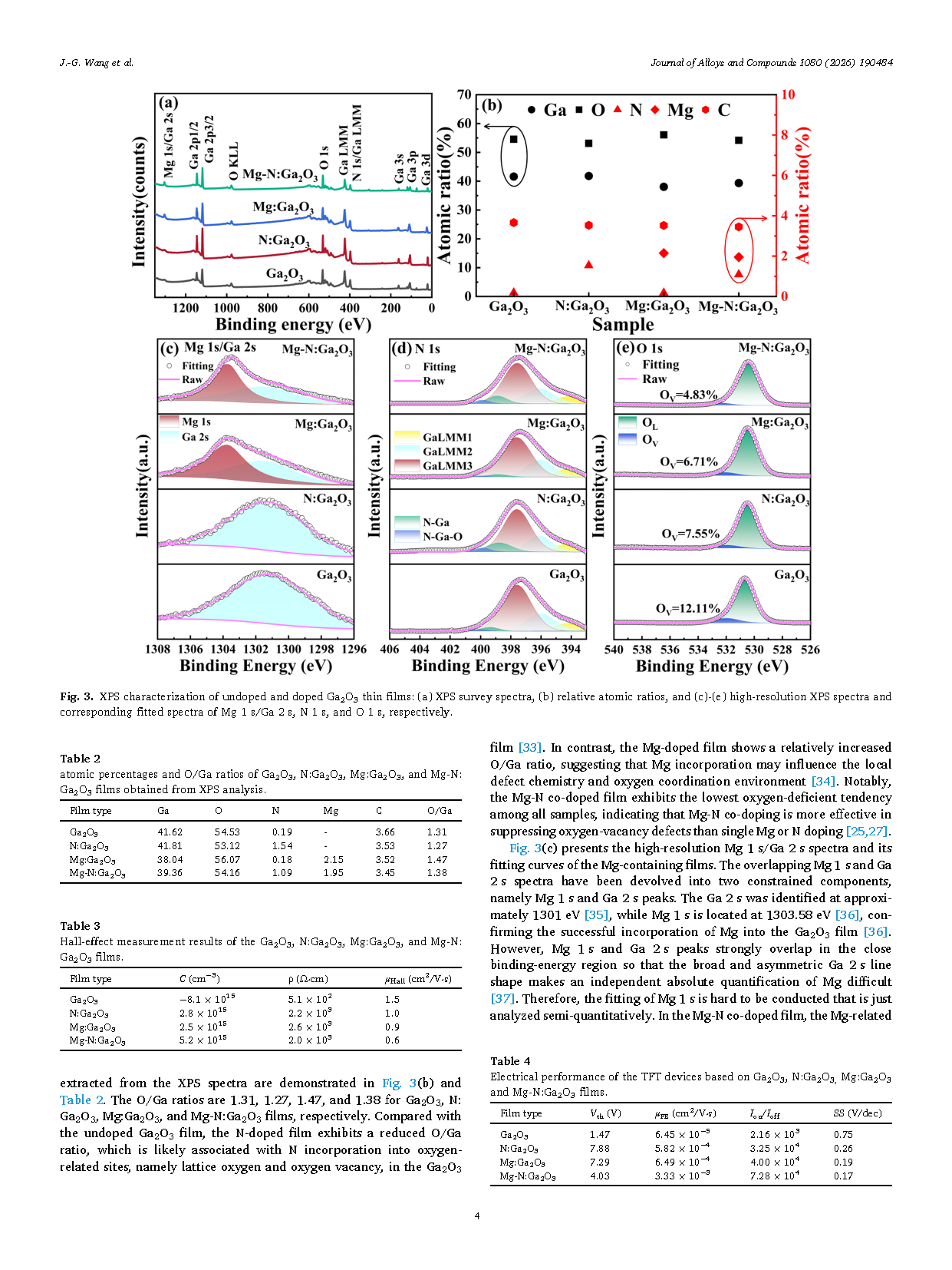
Fig. 3 XPS characterization of undoped and doped Ga₂O₃ thin films: (a) XPS survey spectra, (b) relative atomic ratios, and (c)-(e) high-resolution XPS spectra and corresponding fitted spectra of Mg 1s/Ga 2s, N 1s, and O 1s, respectively.
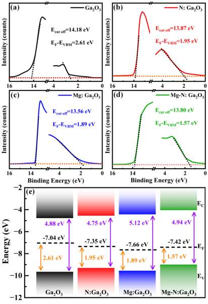
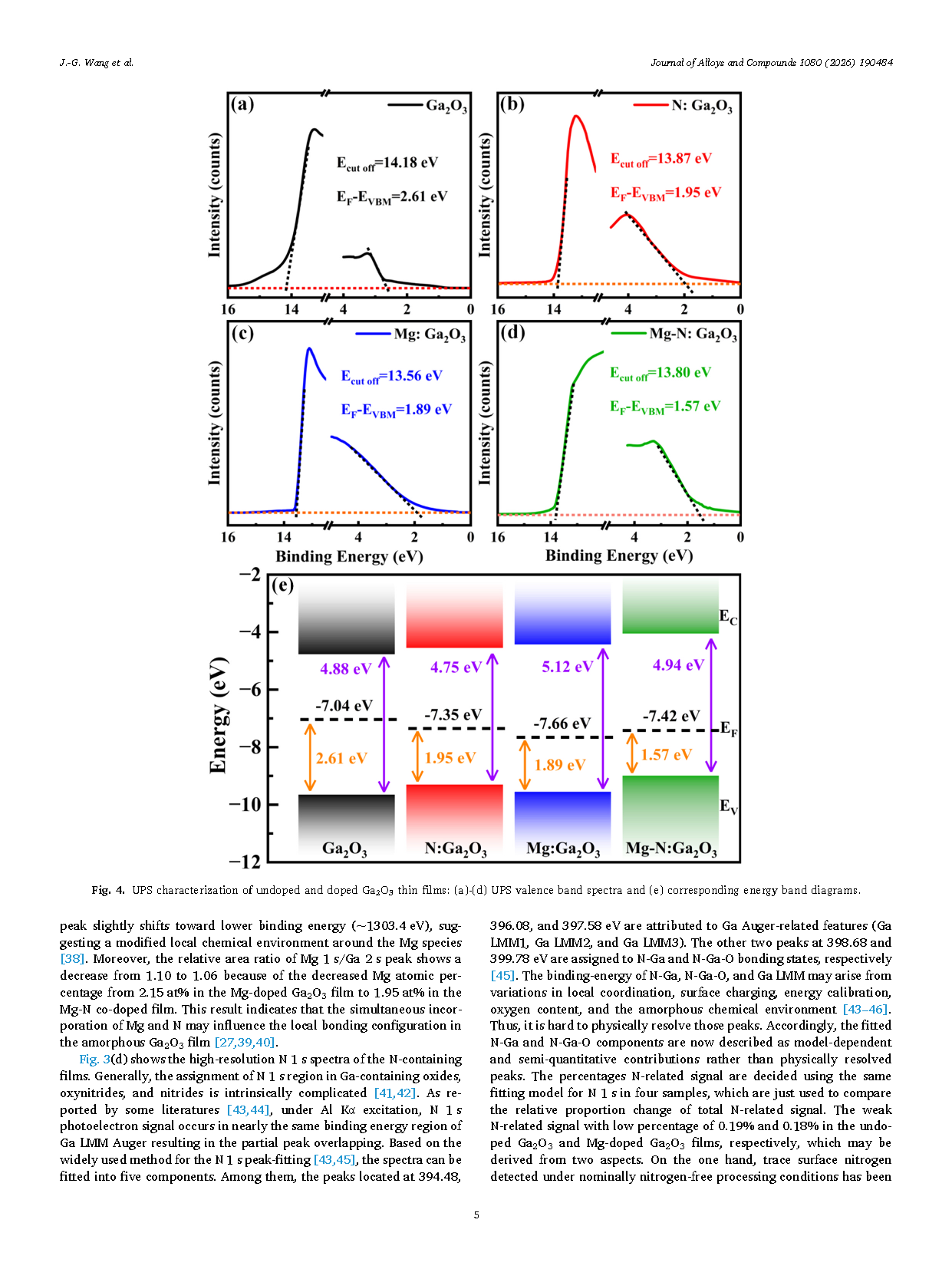
Fig. 4 UPS characterization of undoped and doped Ga₂O₃ thin films: (a)-(d) UPS valence band spectra and (e) corresponding energy band diagrams.
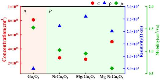
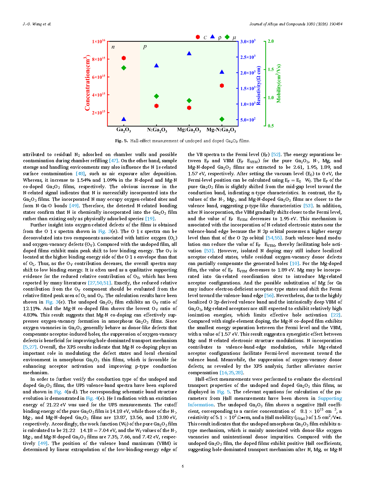
Fig. 5 Hall-effect measurement of undoped and doped Ga₂O₃ films.
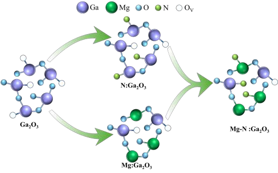
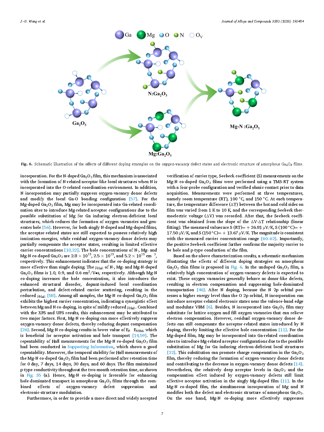
Fig. 6 Schematic illustration of the effects of different doping strategies on the oxygen-vacancy defect states and electronic structure of amorphous Ga₂O₃ films.
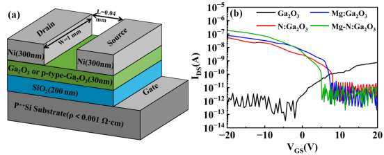
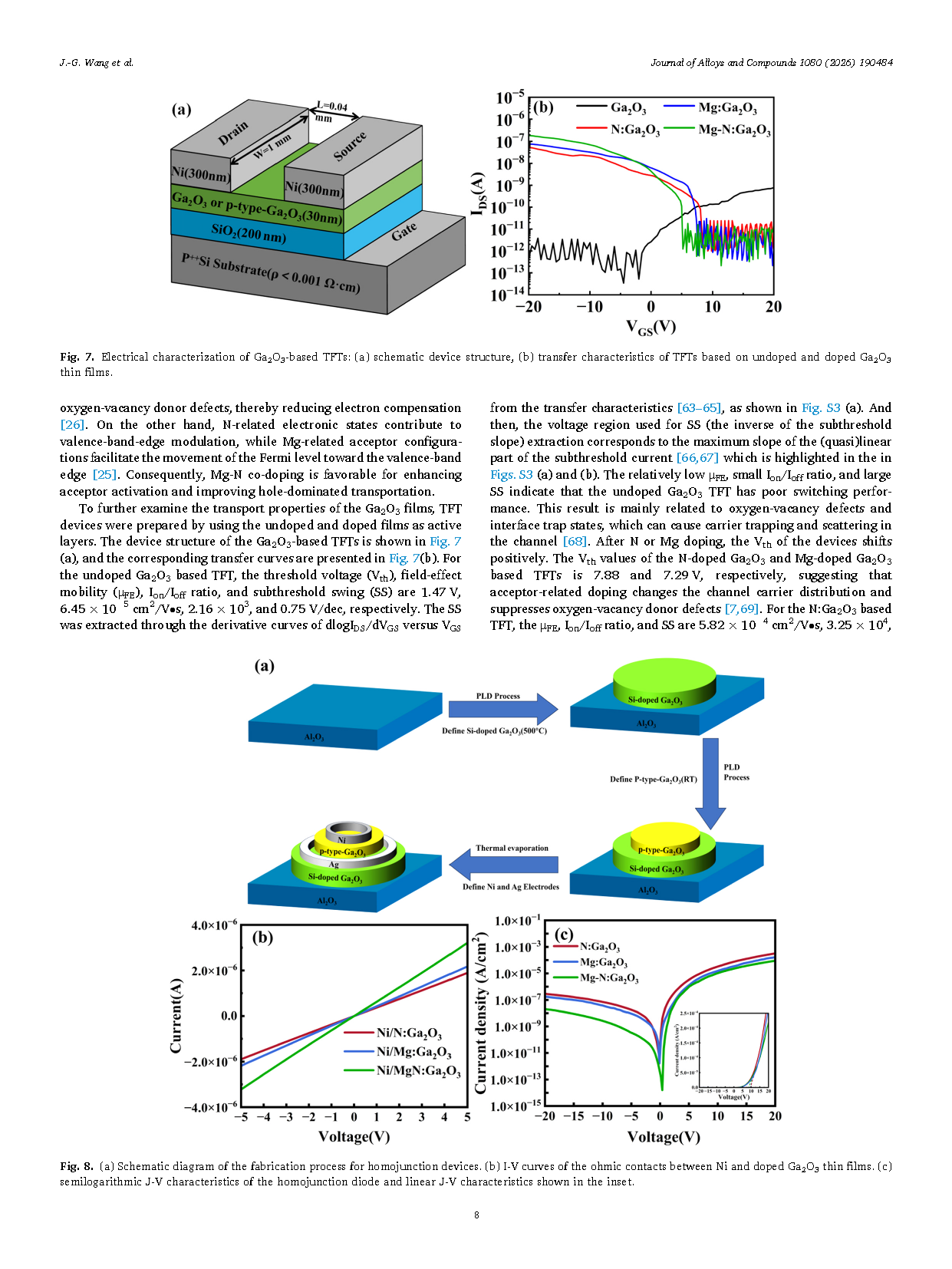
Fig. 7 Electrical characterization of Ga₂O₃-based TFTs: (a) schematic device structure, (b) transfer characteristics of TFTs based on undoped and doped Ga₂O₃ thin films.
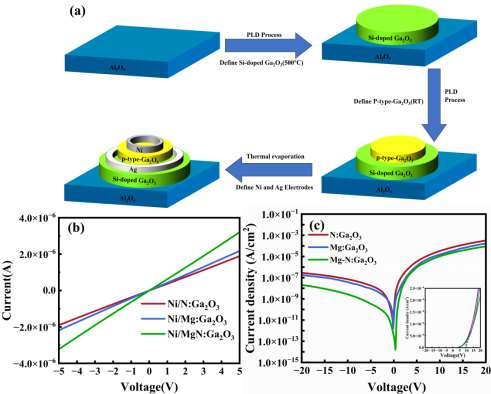
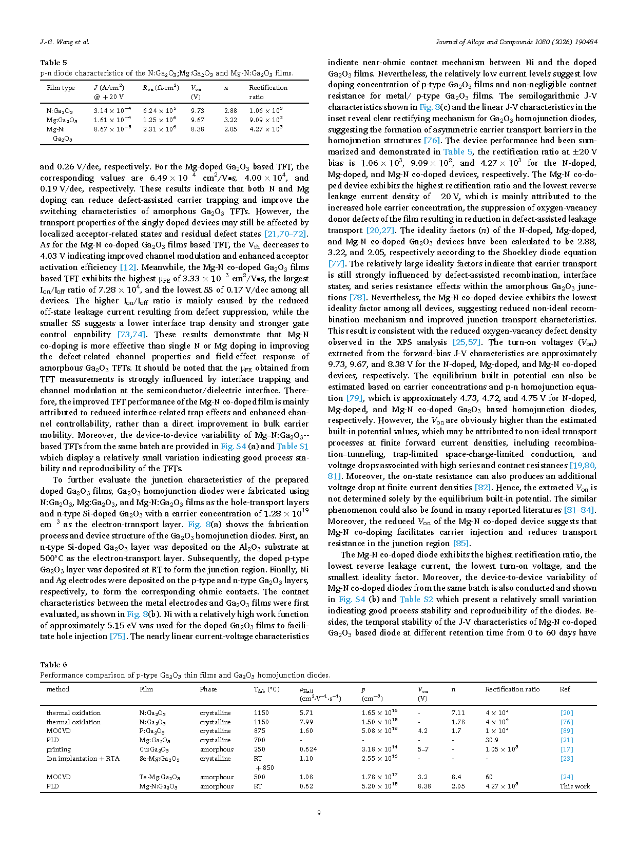
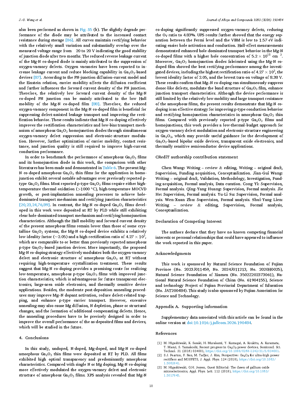
Fig. 8 (a) Schematic diagram of the fabrication process for homojunction devices. (b) I-V curves of the ohmic contacts between Ni and doped Ga₂O₃ thin films. (c) semilogarithmic J-V characteristics of the homojunction diode and linear J-V characteristics shown in the inset.
DOI:
doi.org/10.1016/j.jallcom.2026.190484
Instruction
Official Account

Cooperation
Top
