


Researchers from Hunan University of Science and Engineering, Xiamen University, Hunan University, Jishou University have published a dissertation titled "Machine learning and first-principles calculations for electronic and transport properties in p-type Cd-doped two-dimensional Ga₂O₃" in Journal of Physics D: Applied Physics.
Background
Two-dimensional β-Ga₂O₃ inherits the ultra-wide bandgap advantages of bulk materials, and meanwhile exhibits dimensional confinement effect and large specific surface area, showing broad application prospects in nanoscale optoelectronic devices. Considerable progress has been achieved on n-type doping of two-dimensional Ga₂O₃, nevertheless, the p-type doping bottleneck severely hinders its device implementation. The valence band maximum features relatively flat orbitals, and acceptor impurities tend to form deep-level acceptor states, making effective hole conduction difficult to realize. Existing theoretical works have screened potential p-type dopants including Mg, Zn and Cd. Among them, Cd doping presents obvious Fermi-level downward shift and low activation energy, but most relevant investigations focus on three-dimensional bulk systems. Two-dimensional Ga₂O₃ is obtained via mechanical exfoliation by breaking Ga-O bonds, its atomic arrangement differs evidently from three-dimensional counterparts, and conclusions for bulk phases cannot be directly extrapolated to 2D cases. At present, systematic quantitative investigations on band engineering, hole transport and thermal transport properties for Cd-doped two-dimensional Ga₂O₃ are insufficient. Besides, the application of machine-learning atomic potentials for thermal-transport simulation of this 2D doped system remains to be verified. Such research gap restricts the design and development of two-dimensional p-type Ga₂O₃ materials.
Abstract
Addressing the p-type doping bottleneck in 2D Ga₂O₃ remains a crucial challenge for advancing next-generation electronics. In this study, we employ Heyd–Scuseria–Ernzerhof hybrid density functional calculation to reveal that the p-type conductivity of 2D Cd-doped Ga₂O₃ (CdGaI) originates from the strongly hybridization between Cd-4dxy and O-2p states at the valence band maximum (VBM), while retaining a direct bandgap feature. The enhanced VBM band curvature reduces the hole effective mass and yields an ultrahigh hole mobility of ~ 417.68 cm² V⁻¹ s⁻¹, accompanied by a pronounced mobility anisotropy of 34.86. Using the highly efficient neuroevolution potential-based machine learning, the calculated lattice thermal conductivity of CdGaI is decreased by ∼30% compared with that of perfect 2D Ga₂O₃. This can be attributed to the increased atomic mass of Cd and enhanced scattering of low-frequency acoustic and optical phonons, both of which shorten the phonon mean free path. Temperature-dependent lattice thermal conductivity follows a power law behavior of ~ T-1.3 along the x direction, indicating combined three-phonon and four-phonon scattering processes, whereas ~ T-1.1 along the y direction, where three-phonon scattering dominate. Particularly, CdGaI structure with −2% compressive strain exhibits the robust p-type conductivity, direct bandgap, ultra-high hole mobility and anisotropy, underlining its strong potential for optoelectronic device applications.
Highlights
Hybrid HSE functional calculations reveal that p-type conduction of Cd-doped 2D Ga₂O₃originates from strong hybridization between Cd-4dxy and O-2p states at VBM with direct bandgap maintained.
Obtain ultra-high hole mobility of ~ 417.68 cm² V⁻¹s⁻¹ and large mobility anisotropy for unstrained CdGaI from deformation potential theory.
NEP-ML simulations show that lattice thermal conductivity of CdGaIis reduced by ~30%, and anisotropic phonon scattering mechanisms along x / y directions are clarified.
−2% compressive-strained CdGaIsimultaneously realizes robust p-type conductivity, direct bandgap, high hole mobility and transport anisotropy for optoelectronic applications.
Conclusion
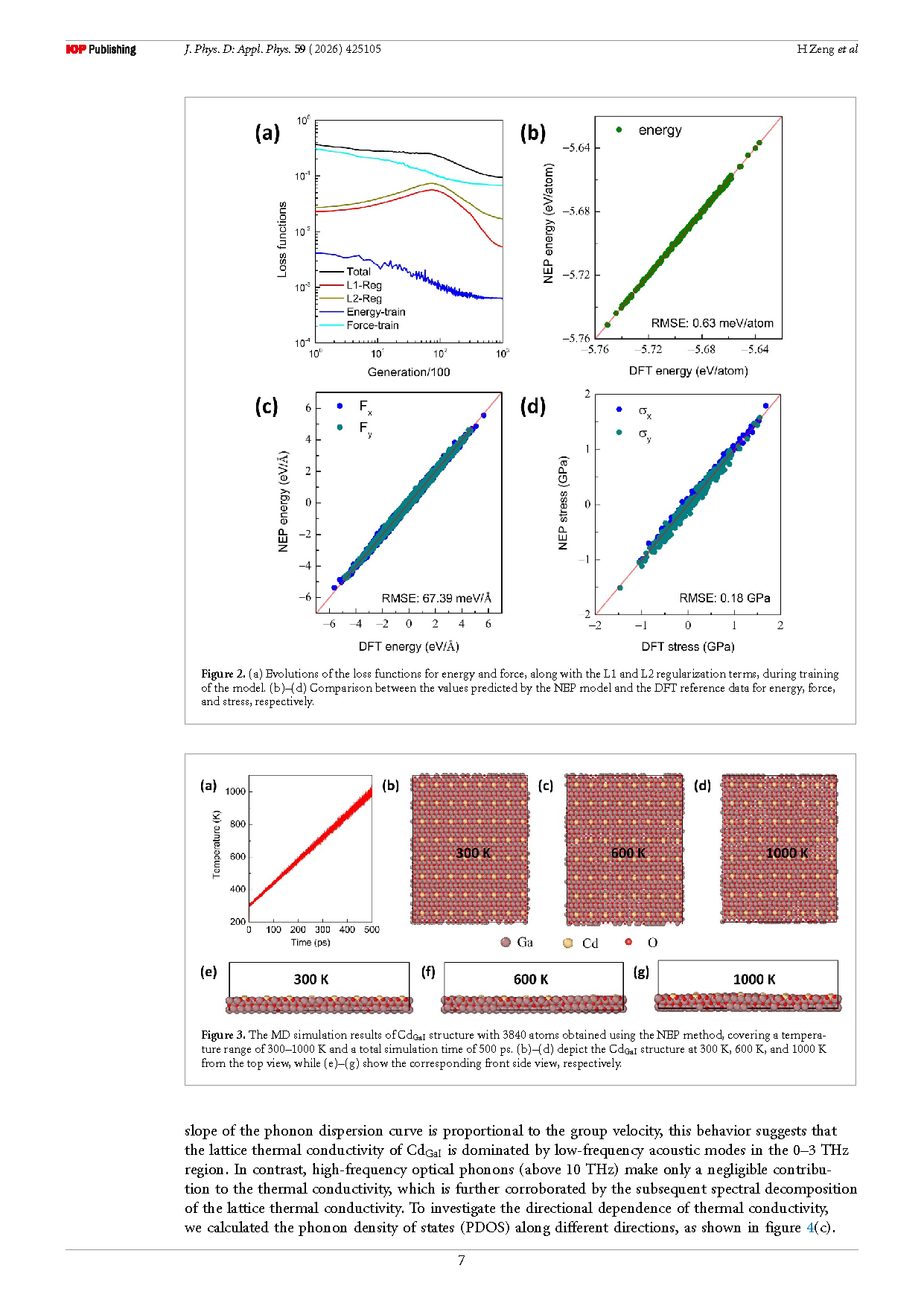
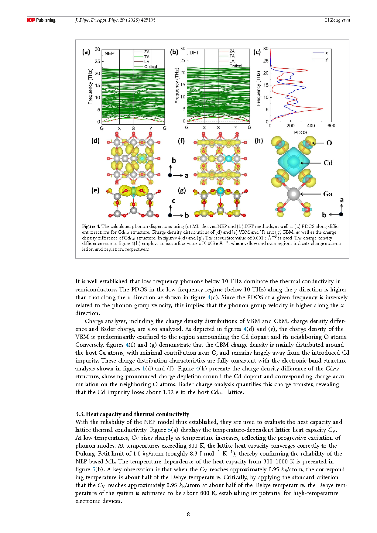
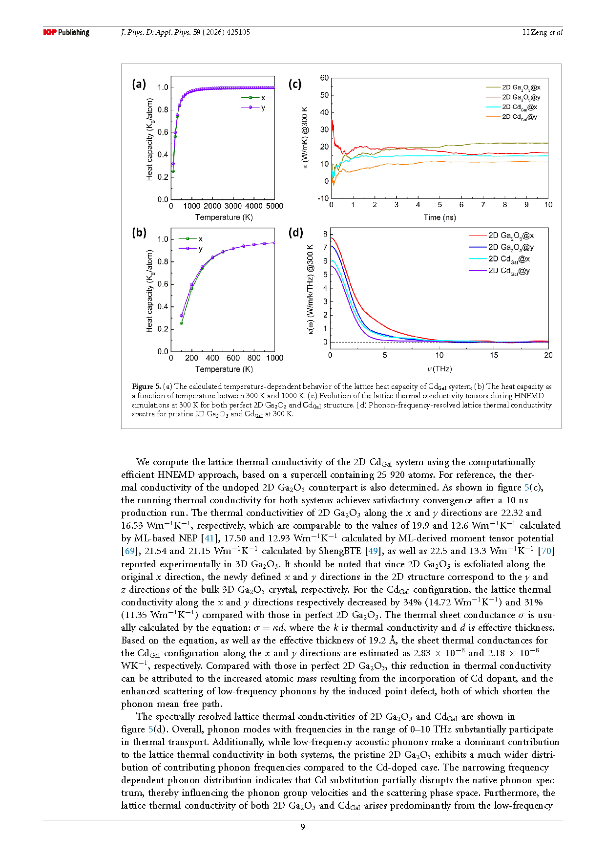
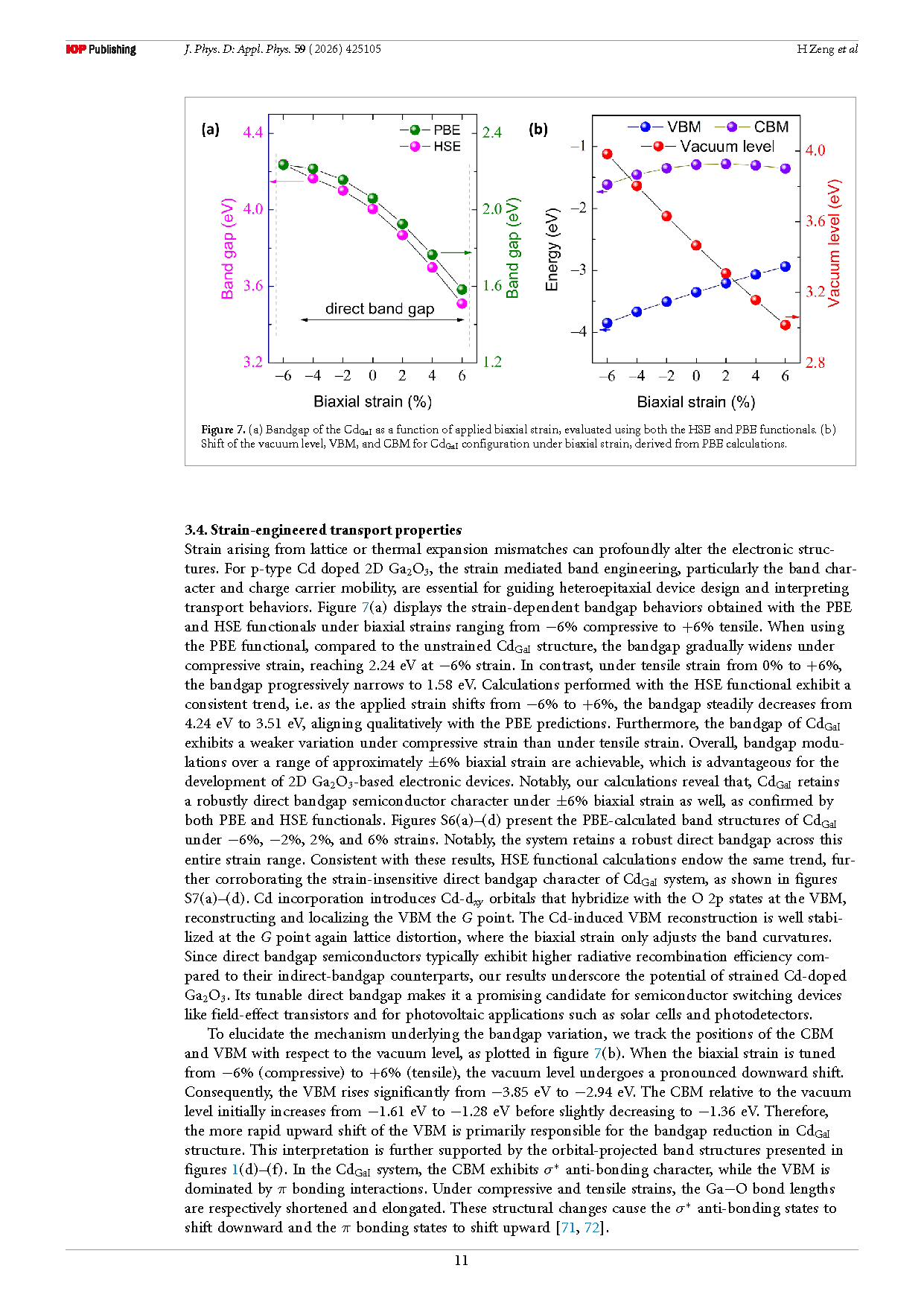
Using first-principles and ML NEP methods in conjunction with DP theory, the detailed structural stability, electronic properties, lattice thermal transport, and carrier mobilities of Cd-doped 2D Ga₂O₃ are explored. Our result indicate that the foreign Cd preferentially substitute at the GaI site, especially under the O-rich condition. The thermodynamic and dynamic stabilities of CdGaI structure are further corroborated by the MD simulations and phonon dispersion analyses, respectively. Charge analysis demonstrates that the charge density of the VBM is predominantly by the Cd dopant and its neighboring O atoms, while the CBM is mainly distributed around the host Ga atoms and a minor contribution of O. Moreover, charge density difference and Bader charge analysis illustrate pronounced charge depletion around the Cd dopant and the lost electron is about 1.32 e. Comparisons between the ML-NEP predictions and DFT reference values for energy, force, and stress display consistently strong correlations. NEP-based phonon dispersion shows a relatively steep slope within the 0–3 THz range, which gradually becomes flatter at higher frequencies. In the low-frequency regime (below 10 THz), the PDOS along the y direction is higher than that along the x direction, indicating that the thermal conductivity along the x direction is greater than that along the y direction. The Debye temperature of the system is estimated to be about 800 K based on the temperature-dependent behavior of the lattice heat capacity. Notably, our calculations reveal that under ±6% biaxial strain, CdGaI retains a robustly direct bandgap character. The bandgap steadily varies from 4.24 eV to 3.51 eV because of the faster upward movement of the VBM relative to the CBM.
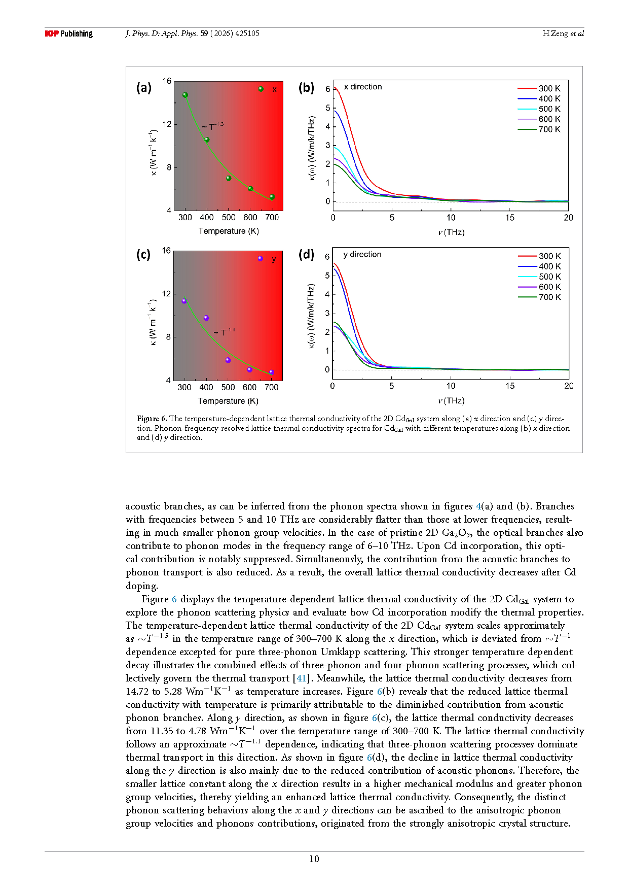
Compared with pristine 2D Ga₂O₃, the lattice thermal conductivities of CdGaI configuration are decreased from 22.32 to 14.72 and from 16.53 to 11.35 Wm⁻¹ K⁻¹ along the x and y directions, respectively. This reduction can be attributed to the increased atomic mass upon Cd incorporation and the enhanced scattering of low-frequency phonons by the induced point defect, both of which shorten the phonon mean free path. Spectrally resolved lattice thermal conductivity further demonstrates that low-frequency acoustic phonons make a dominant contribution to the lattice thermal conductivity. The contribution from the acoustic branches to phonon transport is also reduced upon Cd incorporation.
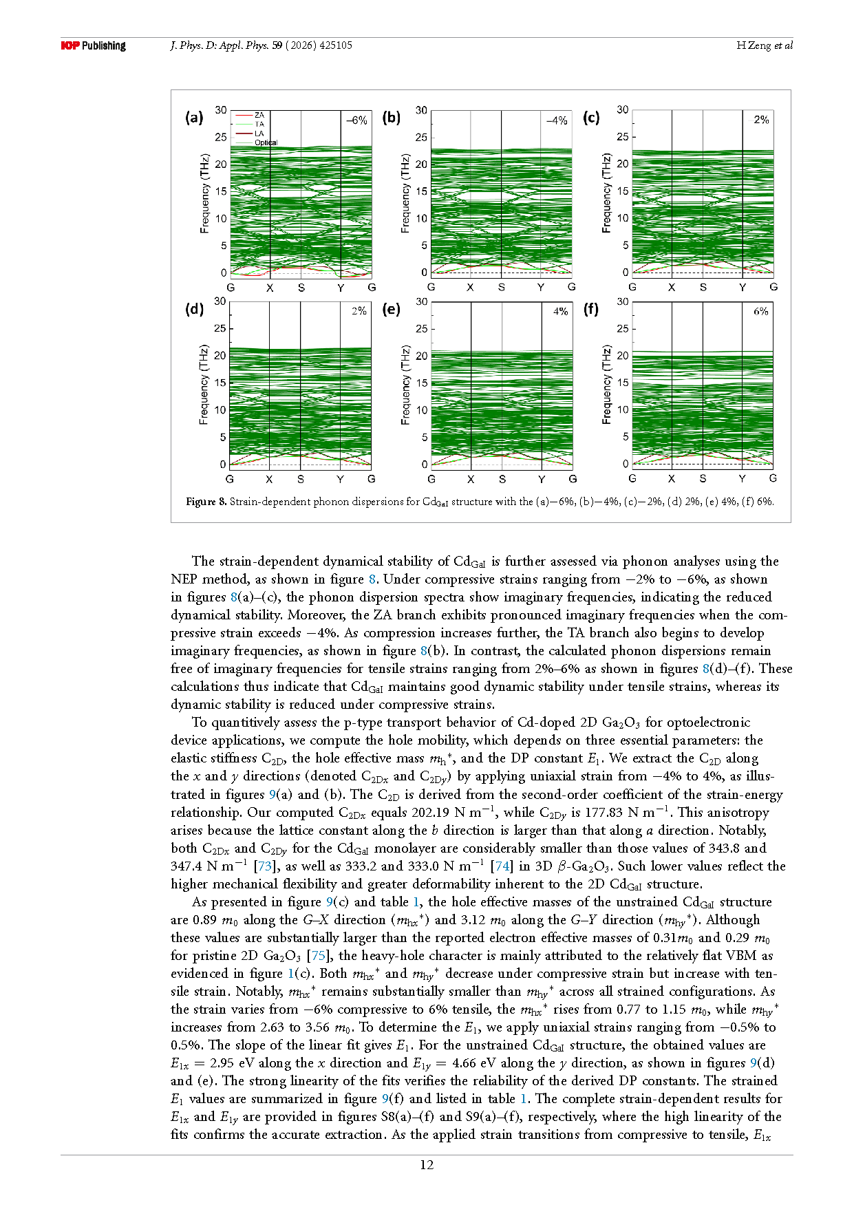
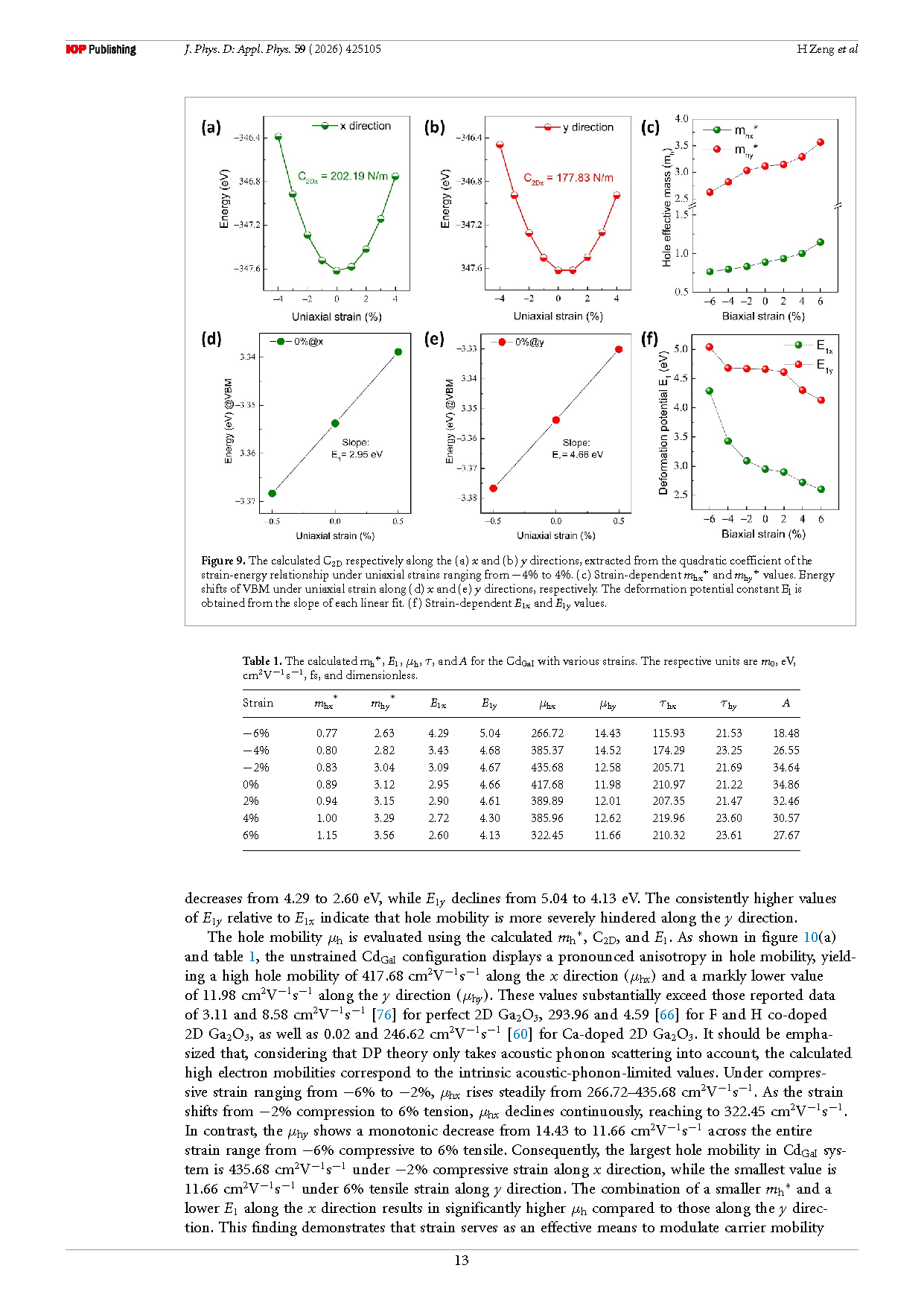
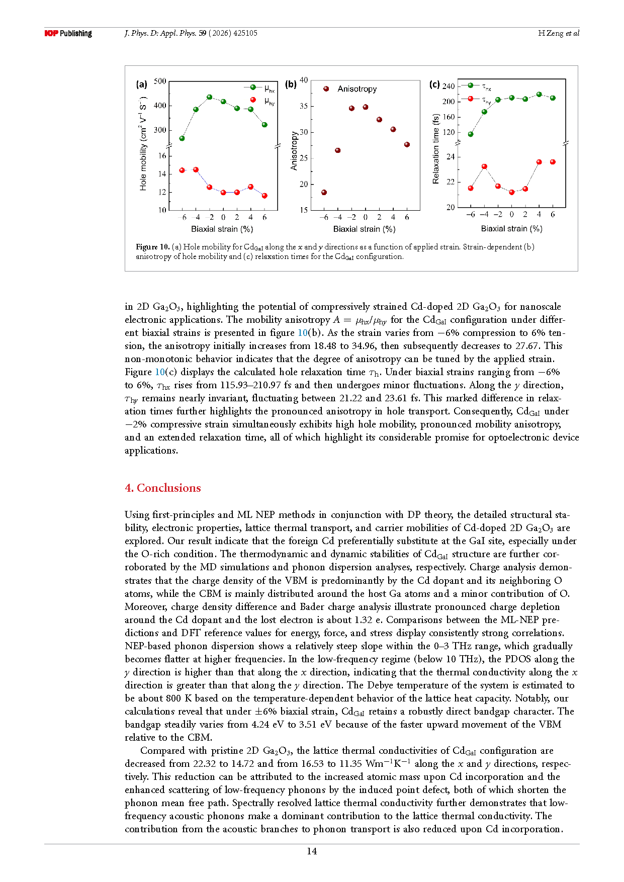
The lattice thermal conductivity decreases from 14.72 to 5.28 Wm⁻¹ K⁻¹ as temperature increases from 300 to 700 K along x direction (following a ~ T-1.3 trend), which indicates that both three-phonon and four-phonon scattering processes govern the thermal transport. Along y direction, it decreases from 11.35 to 4.78 Wm⁻¹ K⁻¹ and follows an approximate ~ T-1.1 dependence, indicating that three-phonon scattering process dominates. Moreover, the decline in lattice thermal conductivity along the y direction is also associated with a reduced contribution of acoustic phonons. Strain-dependent phonon dispersions show that the CdGaI structure maintains good dynamic stability under tensile strain, whereas its dynamic stability is reduced under compressive strain. The μhx and μhy are respectively 417.68 cm² V⁻¹ s⁻¹ and 11.98 cm² V⁻¹ s⁻¹ for unstrained case. As the strain moves from −6% compression to 6% tension, μhx increases steadily from 266.72-435.68 cm² V⁻¹ s⁻¹ and declines continuously to 322.45 cm² V⁻¹ s⁻¹ along the x direction, while μhy shows a monotonic decrease from 14.43 to 11.66 cm² V⁻¹ s⁻¹ along the y direction. Meanwhile, the anisotropy initially increases from 18.48 to 34.86, then decreases to 27.67. In summary, CdGaI under -2% compressive strain shows simultaneously robust P-type conductivity, a direct bandgap, ultra-high hole mobility and strong transport anisotropy, underlining its considerable potential for optoelectronic device applications.
Project Support
This project was funded by the Natural Science Foundation of Hunan Province (Grant No. 2024JJ7200) and the Fundamental Research Funds for Central Universities (Grant No. 20720240147), Scientific Research Foundation of Hunan Provincial Education Department (Grant No. 25A0590), as well as the Open Fund Project of the Key Laboratory of Computational and Applied New Functional Materials in Hunan Provincial Universities (Grant No. 202507).
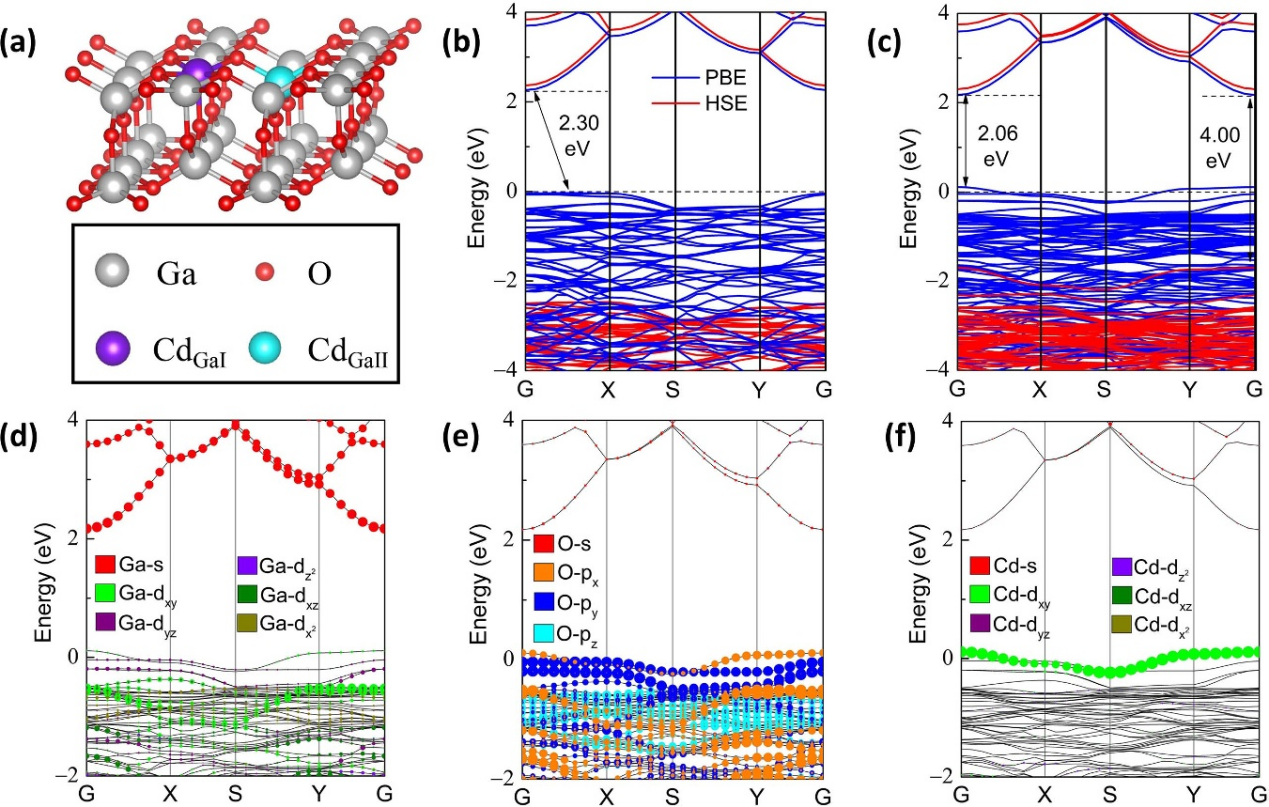
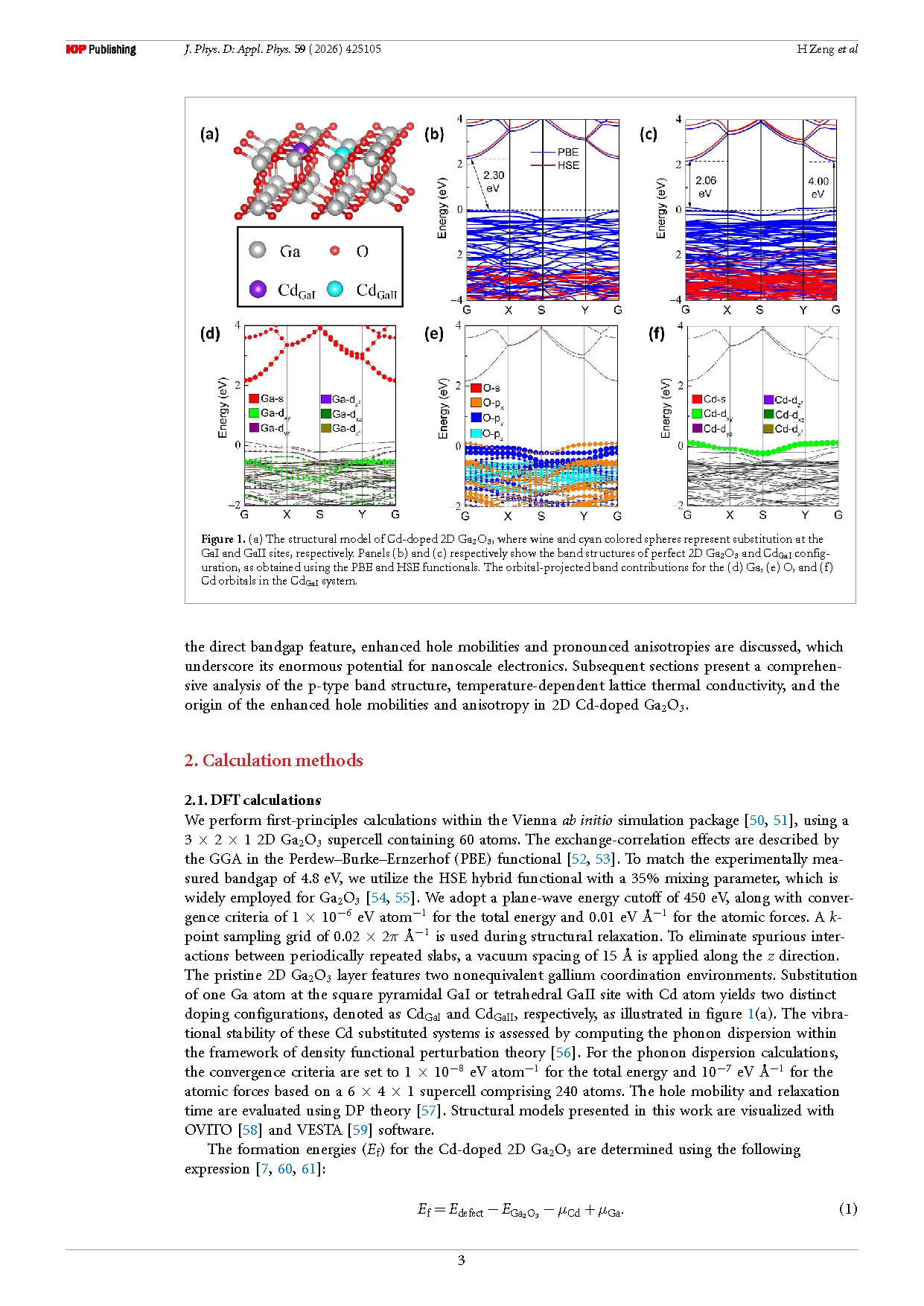
Figure 1. (a) The structural model of Cd-doped 2D Ga₂O₃, where wine and cyan colored spheres represent substitution at the GaI and GaII sites, respectively. Panels (b) and (c) respectively show the band structures of perfect 2D Ga₂O₃ and CdGaI configuration, as obtained using the PBE and HSE functionals. The orbital-projected band contributions for the (d) Ga, (e) O, and (f) Cd orbitals in the CdGaI system.
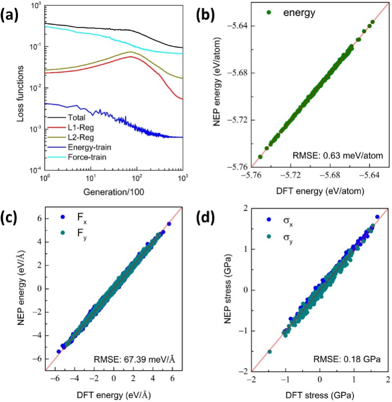
Figure 2. (a) Evolutions of the loss functions for energy and force, along with the L1 and L2 regularization terms, during training of the model. (b)–(d) Comparison between the values predicted by the NEP model and the DFT reference data for energy, force, and stress, respectively.
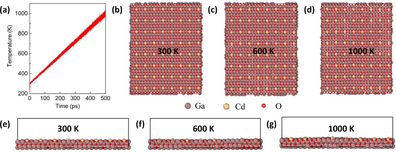
Figure 3. The MD simulation results of CdGaI structure with 3840 atoms obtained using the NEP method, covering a temperature range of 300–1000 K and a total simulation time of 500 ps. (b)–(d) depict the CdGaI structure at 300 K, 600 K, and 1000 K from the top view, while (e)–(g) show the corresponding front side view, respectively.
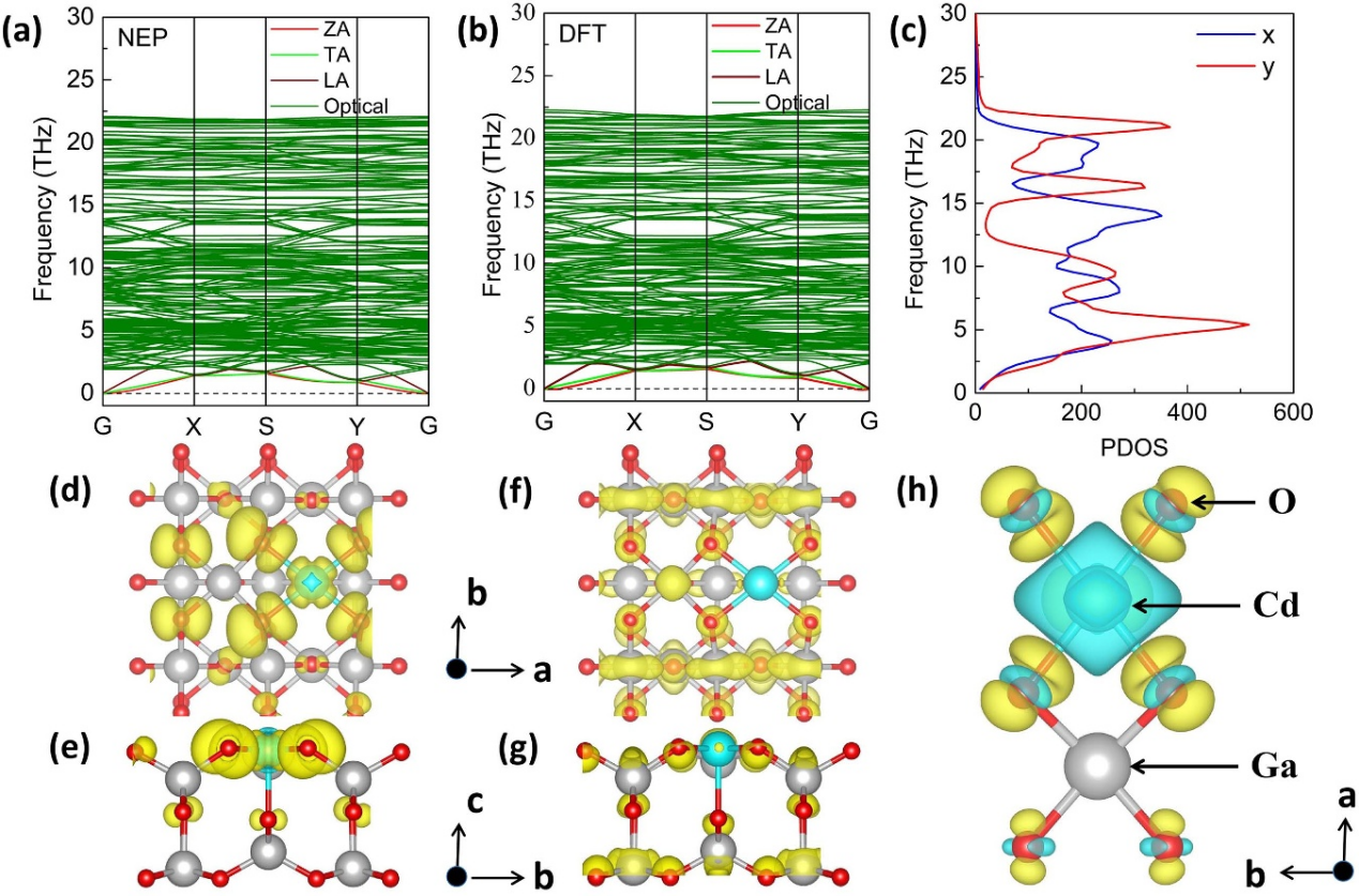
Figure 4. The calculated phonon dispersions using (a) ML-derived NEP and (b) DFT methods, as well as (c) PDOS along different directions for CdGaI structure. Charge density distributions of (d) and (e) VBM and (f) and (g) CBM, as well as the charge density difference of CdGaI structure. In figures 4 (d) and (g), The isosurface value of 0.001 e Å⁻³ is used. The charge density difference map in figure 4 (h) employs an isosurface value of 0.003 e Å⁻³, where yellow and cyan regions indicate charge accumulation and depletion, respectively.
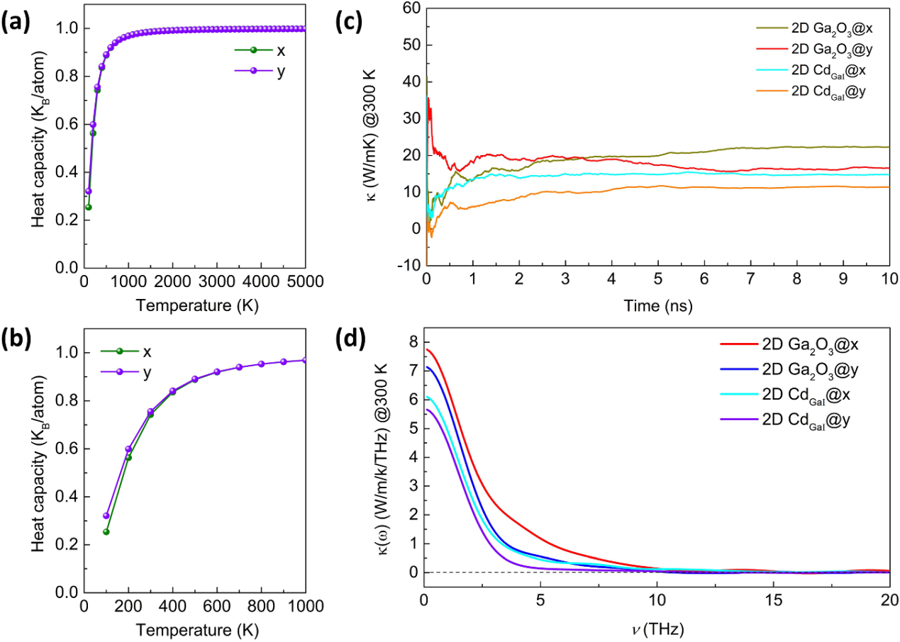
Figure 5. (a) The calculated temperature-dependent behavior of the lattice heat capacity of CdGaI system, (b) The heat capacity as a function of temperature between 300 K and 1000 K. (c) Evolution of the lattice thermal conductivity tensors during HNEMD simulations at 300 K for both perfect 2D Ga₂O₃ and CdGaI structure. (d) Phonon-frequency-resolved lattice thermal conductivity spectra for pristine 2D Ga₂O₃ and CdGaI at 300 K.
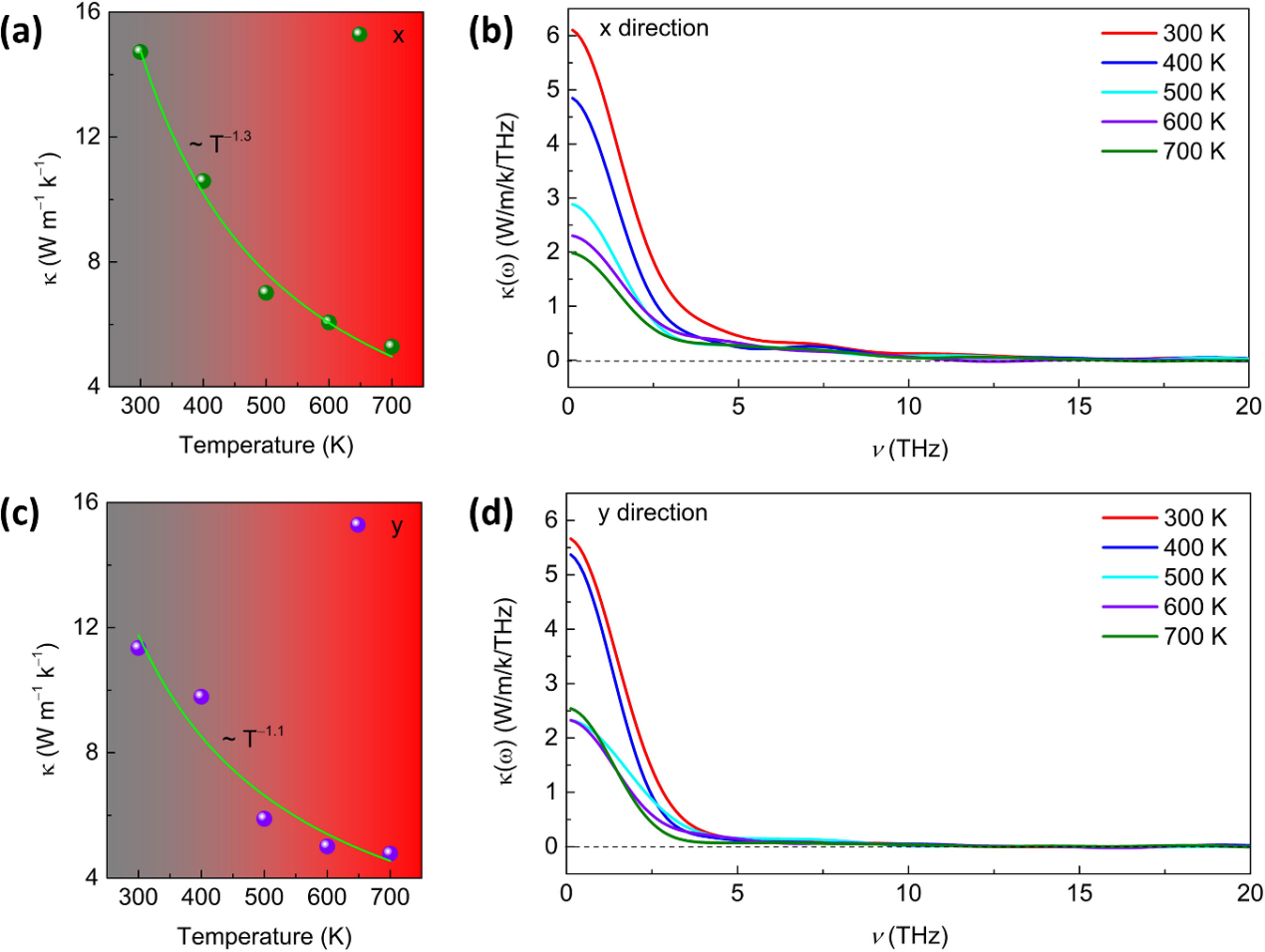
Figure 6. The temperature-dependent lattice thermal conductivity of the 2D CdGaI system along (a) x direction and (c) y direction. Phonon-frequency-resolved lattice thermal conductivity spectra for CdGaI with different temperatures along (b) x direction and (d) y direction.
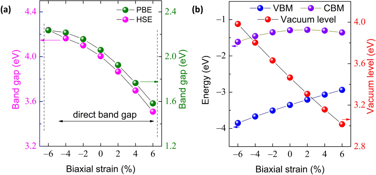
Figure 7. (a) Bandgap of the CdGaI as a function of applied biaxial strain, evaluated using both the HSE and PBE functionals. (b) Shift of the vacuum level, VBM, and CBM for CdGaI configuration under biaxial strain, derived from PBE calculations.
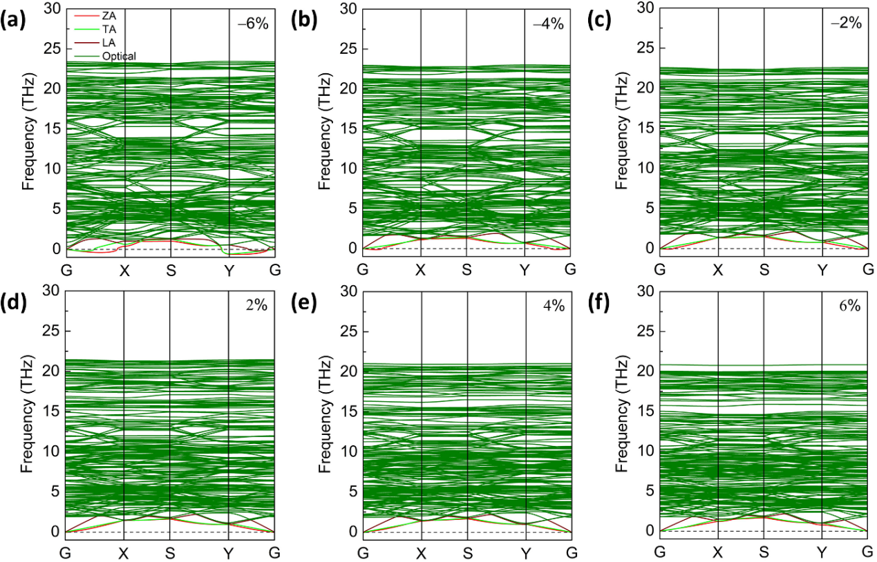
Figure 8. Strain-dependent phonon dispersions for CdGaI structure with the (a)−6%, (b)−4%, (c)−2%, (d) 2%, (e) 4%, (f) 6%.
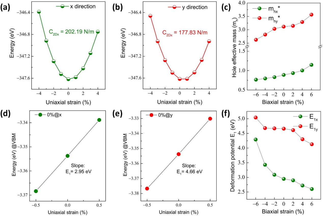
Figure 9. The calculated C2D respectively along the (a) x and (b) y directions, extracted from the quadratic coefficient of the strain-energy relationship under uniaxial strains ranging from −4% to 4%. (c) Strain-dependent mhx* and mhy* values. Energy shifts of VBM under uniaxial strain along (d) x and (e) y directions, respectively. The deformation potential constant E₁ is obtained from the slope of each linear fit. (f) Strain-dependent E1x and E1y values.
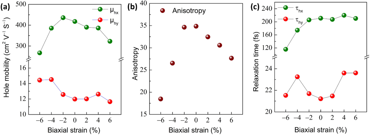
Figure 10. (a) Hole mobility for CdGaI along the x and y directions as a function of applied strain. Strain-dependent (b) anisotropy of hole mobility and (c) relaxation times for the CdGaI configuration.
DOI:
doi.org/10.1088/1361-6463/aeb30e
Instruction
Official Account

Cooperation
Top
