


Researchers from Northeast Normal University and Inner Mongolia University have published a paper titled "Unveiling Surface-Vacancy-Mediated Negative Photoconductivity in γ-Ga₂O₃ Quantum Dots for Solar-Blind Inhibitory Optoelectronic Synapses and In-Sensor Computing" in Laser & Photonics Reviews.
Background
Conventional optoelectronic synapses predominantly emulate excitatory neuronal functions via positive photoconductivity, leaving the equally critical inhibitory signaling largely underexplored and vulnerable to visible‑light interference. Solar‑blind ultraviolet detection (response wavelength shorter than 280 nm) is attractive for fingerprint recognition, flame monitoring and secure optical communication. Gallium oxide (Ga₂O₃) features an ultra‑wide bandgap of ∼4.9 eV and intrinsic solar‑blind selectivity without external optical filters. Oxygen vacancy (Vₒ) defects in Ga₂O₃ act as programmable charge‑trapping centers for synaptic weight modulation. Nevertheless, bulk, thin‑film and one‑dimensional Ga₂O₃ suffer from low surface‑to‑volume ratio, most Vₒ defects are buried inside bulk and hardly participate in interfacial charge exchange. Zero‑dimensional quantum dots possess ultrahigh specific surface area to expose abundant surface‑active Vₒ, yet pure quantum‑dot assemblies suffer from poor carrier transport and weak photocurrent. Hybrid architectures combining γ‑Ga₂O₃ quantum dots with high‑mobility graphene enable quantum dots to work as surface‑charge‑sensitive gate to modulate graphene channel conductance. In this work, γ‑Ga₂O₃ QDs/graphene heterojunctions with tunable Vₒ concentration are systematically investigated, the underlying negative photoconductivity mechanism is clarified, and inhibitory synapse and in‑sensor reservoir‑computing fingerprint‑recognition applications are demonstrated.
Abstract
Conventional optoelectronic synapses predominantly emulate excitatory neuronal functions via positive photoconductivity, leaving the equally critical inhibitory signaling largely underexplored and vulnerable to visible‑light interference. Here, we unveil a negative photoconductivity (NPC) in the solar‑blind ultraviolet region, achieved at the shortest reported wavelength of 230 nm, in γ‑Ga₂O₃ quantum dots (QDs)/graphene heterojunctions. The mechanism originates from surface‑active oxygen vacancies (Vₒ) that enable reversible O₂ chemisorption; 230 nm illumination triggers O₂⁻ recombination, driving interfacial electron transfer that suppresses graphene conductance via a photo‑induced gating effect. This NPC physics delivers an ultrahigh responsivity of −8077 A/W and 279 s retention, emulating inhibitory plasticity (paired‑pulse depression, learning‑forgetting‑relearning). Harnessing the same nonlinear dynamics, we construct an in‑sensor reservoir computing system achieving 96% fingerprint recognition accuracy (91% under 30% noise) without preprocessing, far outperforming conventional visible‑light‑based schemes. Given that the ultrahigh specific surface area of the 0D QDs maximizes the fraction of surface‑exposed, chemically active Vₒ defects for efficient interfacial charge exchange, this strategy establishes a 0D defect‑engineering paradigm for noise‑immune solar‑blind neuromorphic hardware.
Highlights
① Solvothermal synthesis time is tuned to realize controllable oxygen‑vacancy concentration in γ‑Ga₂O₃ QDs; average QD size ranges from 2.9‑3.3 nm, and oxygen‑vacancy density decreases with prolonged reaction duration.
② Flexible γ‑Ga₂O₃ QDs/graphene heterostructure is fabricated, and pronounced negative photoconductivity is realized under 230 nm solar‑blind UV illumination; ultrahigh negative responsivity of −8077 A/W and signal retention time of 279 s are achieved.
③ Complete physical picture of NPC is clarified: positive photoconductivity appears under vacuum; in ambient atmosphere, surface Vₒ mediates reversible O₂ chemisorption. Light‑induced O₂⁻ recombination injects electrons to recombine holes in graphene channel and yields conductance‑reduction NPC. In‑situ KPFM, UPS and vacuum‑ambient comparative experiments provide solid evidence.
④ The device emulates diverse biological inhibitory synaptic behaviors including paired‑pulse depression (PPD), pulse‑duration/intensity/count/rate‑dependent plasticity, as well as learning‑forgetting‑relearning Ebbinghaus‑like memory dynamics.
⑤ All‑physical in‑sensor reservoir‑computing system is built utilizing device intrinsic nonlinear dynamics to process fingerprint optical pulse sequences on‑site; recognition accuracy reaches 96% under noise‑free condition and remains 91% under 30% salt‑and‑pepper noise, promising noise‑robust solar‑blind neuromorphic vision hardware.
Conclusion
In summary, we demonstrate a defect‑engineered 0D platform for neuromorphic vision by precisely tuning oxygen vacancies in γ‑Ga₂O₃ QDs via a time‑dependent solvothermal strategy. The ultrahigh specific surface area of the QDs maximizes surface‑exposed Vₒ sites, triggering an oxygen‑adsorption‑mediated NPC effect. This mechanism achieves a record responsivity of −8077 A/W and an exceptional retention time of 279 s, enabling faithful emulation of biological inhibitory functions, including paired‑pulse depression and Ebbinghaus learning‑forgetting dynamics. Capitalizing on this intrinsic nonlinearity and short‑term memory, we construct a solar‑blind UV in‑sensor reservoir computing system that directly processes latent fingerprints at the sensor node. The system delivers 96% accuracy under noise‑free conditions and maintains 91% recognition under 30% salt‑and‑pepper noise, significantly outperforming conventional visible‑light schemes. This work establishes a versatile 0D paradigm for noise‑immune, neuromorphic hardware, bridging the gap between wide‑bandgap defect physics and edge‑intelligent security applications.
Project Support
This work was supported by the National Key Research and Development Program of China (2024YFA1208800), the National Natural Science Foundation of China (Nos. 12474164, 62404038, 62674042), the Continuing Grant of Young Scientists Fund (Type A) from the National Natural Science Foundation of China (No. 52625217), the Fund from Jilin Province (Grant No. SKL202602014JC), the Research Projects of the Education Office of Jilin Province (JJKH20250300KJ).
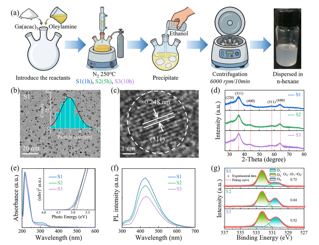
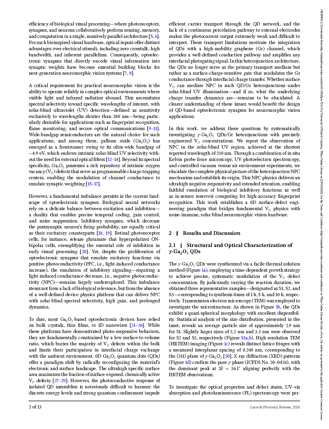
图 1 (a) γ-Ga₂O₃ 量子点溶剂热可控合成流程示意图;(b) S1样品低倍 TEM 图,插图为粒径统计分布;(c) S1 高分辨 TEM 图像,0.248 nm晶格条纹对应 γ-Ga₂O₃ 的(311)晶面;(d) S1/S2/S3三组样品 XRD 谱;(e)紫外‑可见吸收谱与 Tauc 带隙;(f)光致发光PL谱;(g)三组样品 O 1s 的 XPS 高分辨谱,展示OII(氧空位)组分占比随合成时间下降。
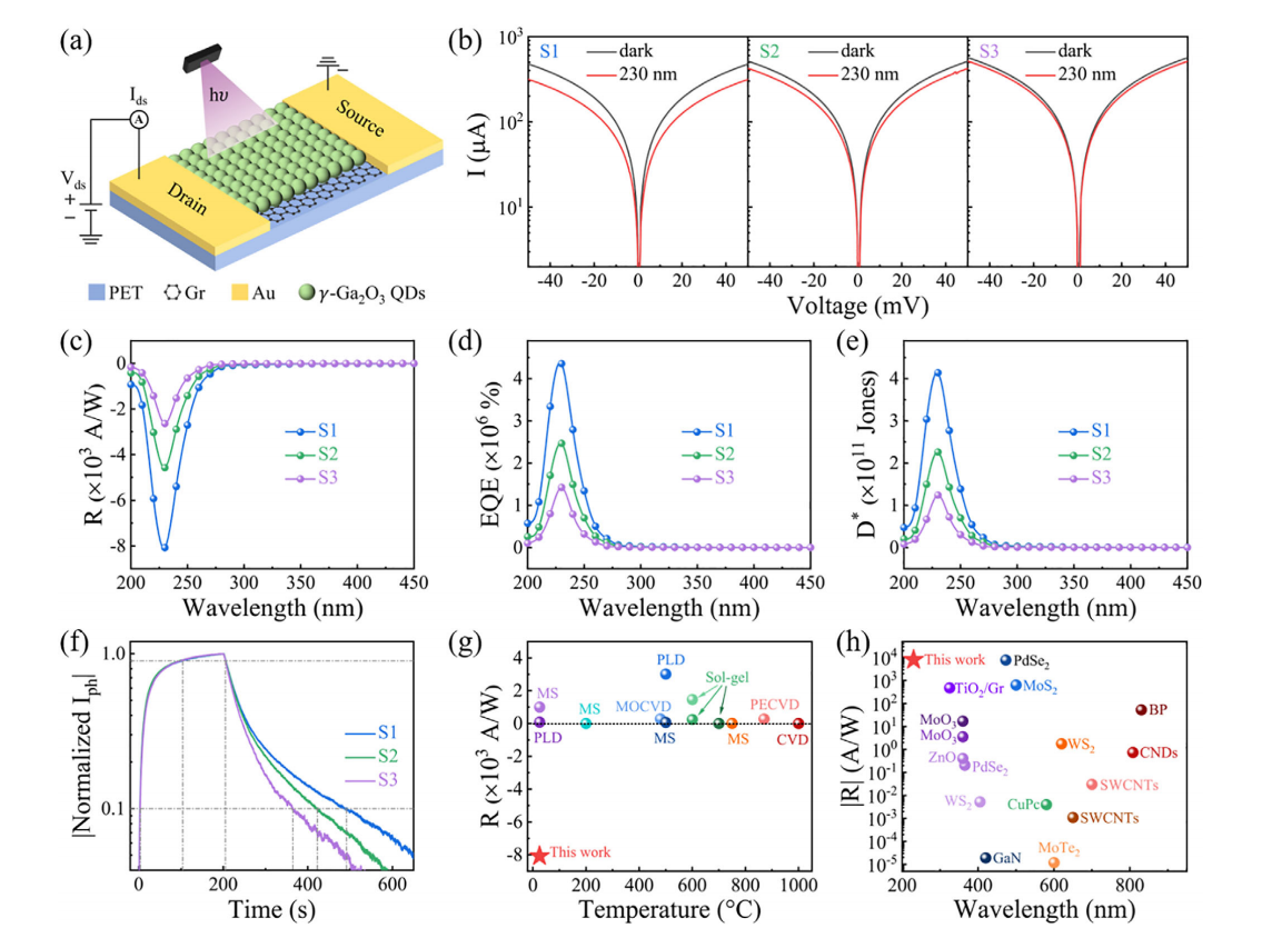
图 2 (a) PET 衬底上 γ-Ga₂O₃ 量子点/石墨烯柔性器件结构示意图;(b) S1/S2/S3 器件暗态与 230 nm光照条件 I‑V 曲线;(c‑e)器件光谱响应性能:(c)响应度 R,(d)外量子效率 EQE,(e)探测率D*;(f)归一化光电流瞬态响应曲线;(g)本器件与已报道 Ga₂O₃ 突触器件的制备温度‑响应度对比;(h)本器件与其他柔性负光电导器件工作波长‑响应度对比。
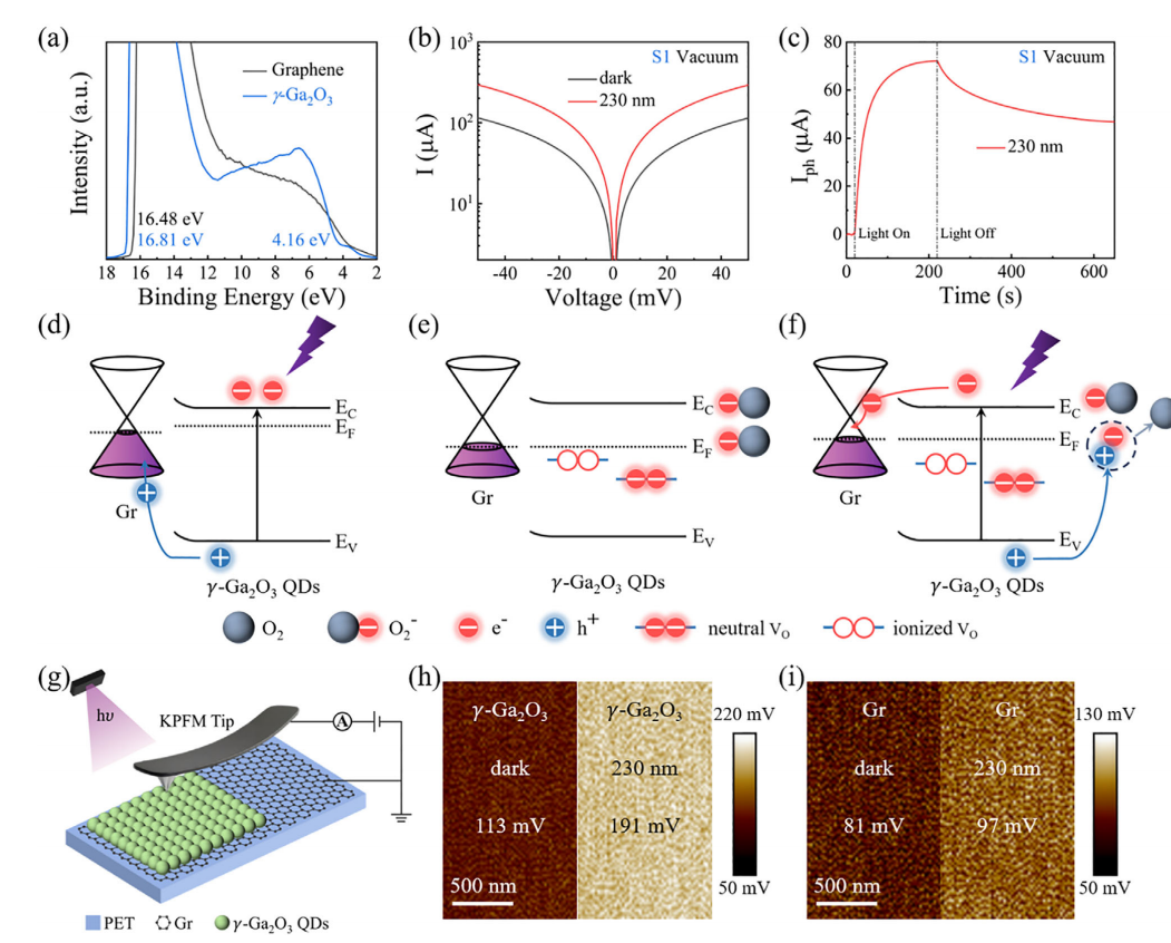
图 3 γ-Ga₂O₃ 量子点/石墨烯器件负光电导工作机理。(a) UPS 谱,分别为 γ-Ga₂O₃ 量子点与石墨烯;(b)真空条件 S1 器件暗态与 230 nm 光照 I‑V 曲线;(c)真空下 I‑t 光电流响应;(d)真空环境正光电导物理示意图;(e)大气环境下氧气在量子点表面吸附示意图;(f)大气光照下负光电导 NPC 机理示意图;(g)原位 KPFM 表面势测试装置示意图;(h) γ-Ga₂O₃ 量子点薄膜暗态与 230 nm 光照表面势 mapping;(i)石墨烯薄膜暗态与 230 nm 光照表面势mapping。
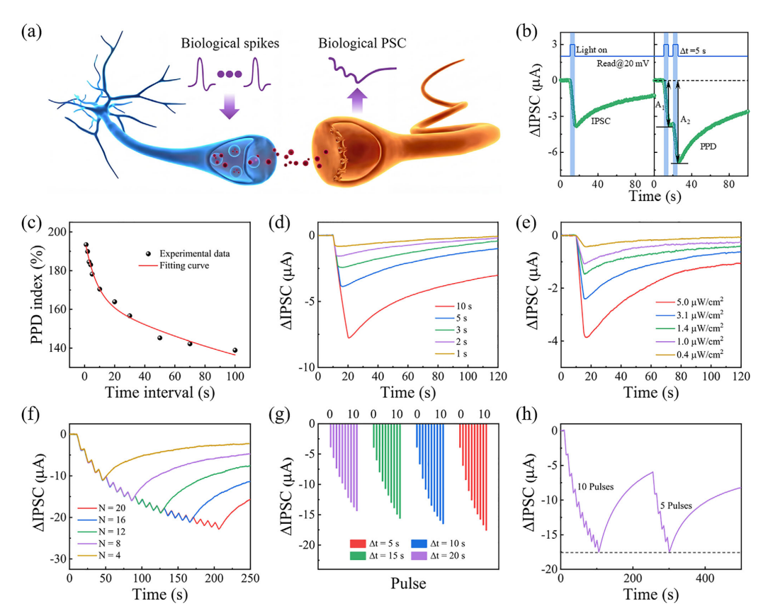
图 4 γ-Ga₂O₃ 量子点/石墨烯异质结仿生抑制型突触特性。(a)生物视网膜抑制突触工作示意图;(b)单光脉冲刺激产生抑制型突触后电流 IPSC,展示成对脉冲抑制 PPD 效应;(c)不同脉冲间隔下 PPD 指数变化;(d)脉冲时长依赖可塑性;(e)光强依赖可塑性;(f)脉冲数目依赖可塑性;(g)脉冲频率依赖可塑性;(h)学习‑遗忘‑再学习动力学曲线。
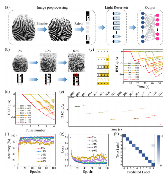
图 5 基于 γ-Ga₂O₃ 量子点/石墨烯光电器件的传感内储备池计算,用于抗噪声指纹识别。(a)指纹图像预处理、编码为4位光脉冲序列输入器件,器件瞬态光电流作为储备池状态,经读出层完成分类识别;(b) 0 %、30 %、60 %椒盐噪声污染后的指纹样本;(c) 16 种 4 位输入脉冲对应的器件瞬态光电流响应;(d)采样得到 16 种可区分储备池状态;(e)重复五次测试的储备池状态稳定性统计;(f)不同噪声条件下识别准确率随训练轮数变化;(g)对应交叉熵损失曲线;(h)无噪声条件下识别混淆矩阵。
DOI:
10.1002/lpor.72112
Instruction
Official Account

Cooperation
Top
