


Researchers from Kyoto Institute of Technology, University of Padua have published a dissertation titled "Epitaxial growth of Si‑doped β‑(InₓGa₁₋ₓ)₂O₃ thin films grown on (010) β‑Ga₂O₃ substrates via mist chemical vapor deposition" in Journal of Applied Physics.
Background
β‑Ga₂O₃ is an ultra‑wide‑bandgap semiconductor with important application value for power devices, and bandgap modulation can be realized by alloying. β‑(InₓGa₁₋ₓ)₂O₃ can tune bandgap toward narrower values and serves as a promising candidate channel‑layer material for β‑Ga₂O₃‑based HEMT devices. MBE and MOCVD vacuum systems can realize epitaxy of such alloy films but suffer high equipment cost. Mist‑CVD is a non‑vacuum technique; alloying and impurity doping can be realized simply by atomizing precursor solutions, featuring high flexibility and low cost. Existing studies mostly focus on growth procedures of this material. Large lattice mismatch under high‑In composition easily triggers strain relaxation and degrades crystal quality and interfacial flatness. Meanwhile, controllable n‑type doping and carrier‑transport scattering mechanisms of β‑(InₓGa₁₋ₓ)₂O₃ remain poorly understood, which limits the adoption of Mist‑CVD‑grown alloys for β‑Ga₂O₃‑based heterostructure device development.
Abstract
In this study, Si‑doped β‑(InₓGa₁₋ₓ)₂O₃ thin films were grown on (010) β‑Ga₂O₃ substrates by mist chemical vapor deposition. The influence of In composition and strain relaxation on the structural and electron transport properties was investigated for β‑Ga₂O₃‑based heterostructure applications. X‑ray diffraction and atomic force microscopy measurements revealed that coherently grown films maintained high crystallinity and smooth surfaces with root mean square roughness values below 1 nm, whereas strain relaxation at high In compositions significantly degraded both crystallinity and surface flatness. Hall effect measurements demonstrated that Si doping enabled carrier concentration control under both coherent growth and strain‑relaxed conditions. Under coherent growth conditions, Hall mobility decreased with increasing In composition despite comparable carrier concentration and crystalline quality, suggesting enhanced alloy disorder scattering associated with random In substitution. Temperature‑dependent Hall measurements revealed degenerate semiconductor behavior with nearly temperature‑independent carrier concentration. Analysis of the temperature‑dependent Hall mobility based on Matthiessen’s rule showed that temperature‑independent scattering (ionized impurity and alloy disorder scattering) accounts for approximately 80% of the total scattering rate even at 300 K, with a phonon‑limited mobility of approximately 240 cm²/Vs. These findings clarify the influence of In composition on the structural and electrical properties of β‑InGaO thin films and provide important insights for β‑Ga₂O₃‑based high‑electron‑mobility heterostructure devices.
Highlights
Realize Si‑doped β‑(InₓGa₁₋ₓ)₂O₃epitaxial thin‑film growth on (010) β‑Ga₂O₃ substrates by non‑vacuum mist‑CVD, and achieve coherent epitaxy with RMS roughness below 1 nm.
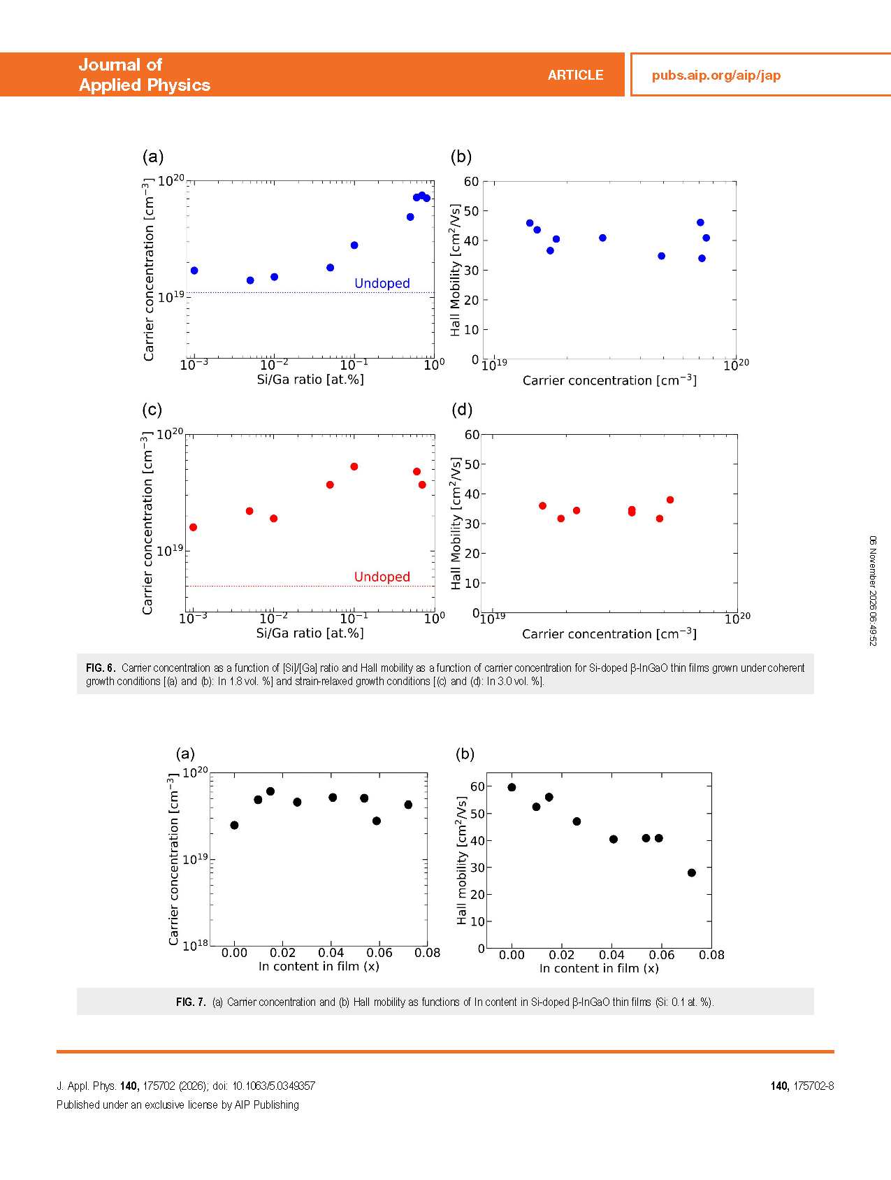
Demonstrate effective carrier‑concentration modulation by Si doping under both coherent‑growth and strain‑relaxed growth conditions.
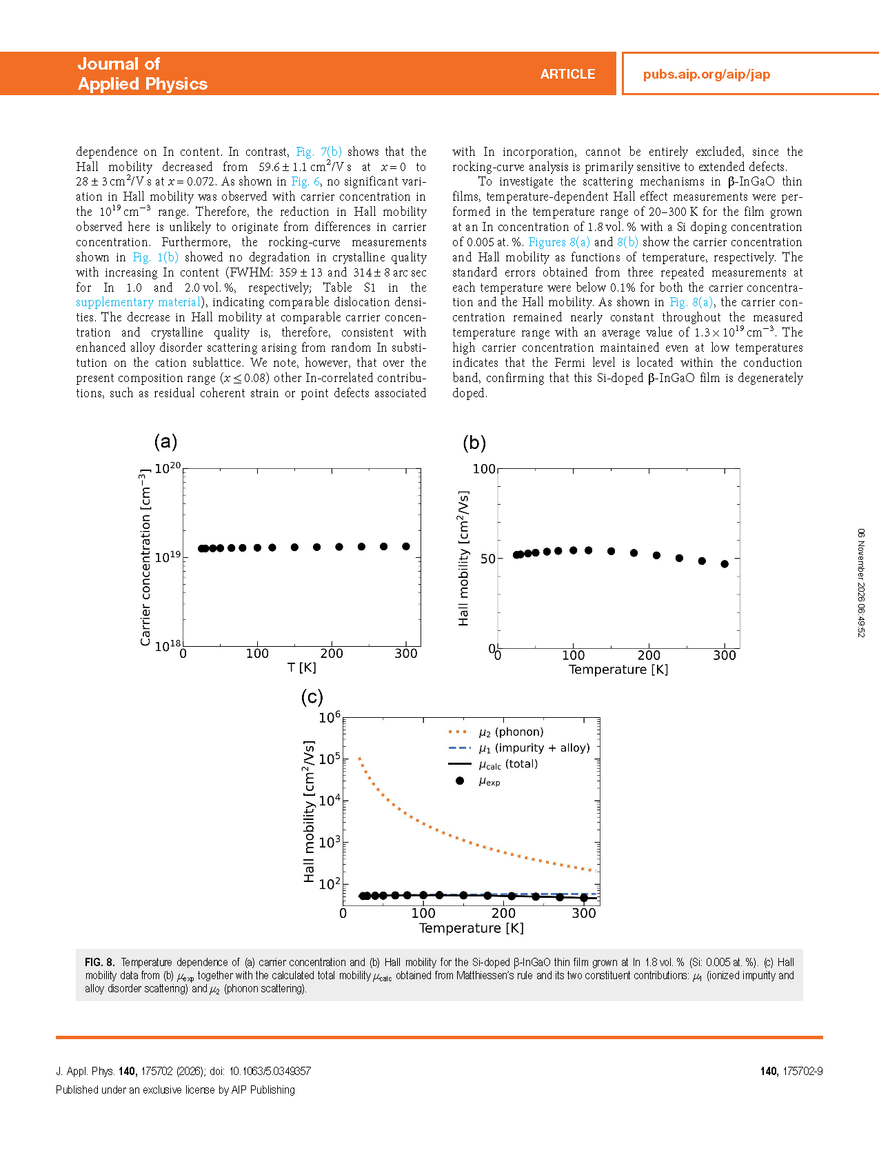
Under coherent‑growth conditions, Hall mobility degrades with increasing In composition at similar carrier concentration and crystal quality, revealing enhanced alloy‑disorder scattering.
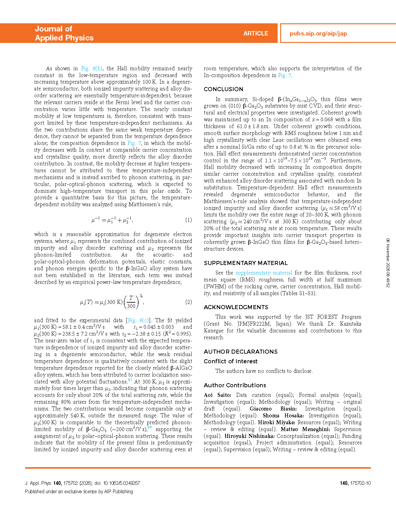
Temperature‑dependent Hall measurement and Matthiessen‑rule analysis quantify scattering contributions; temperature‑independent scattering dominates total scattering rate at room temperature.
Conclusion
In summary, Si‑doped β‑(InₓGa₁₋ₓ)₂O₃ thin films were grown on (010) β‑Ga₂O₃ substrates by mist CVD, and their structural and electrical properties were investigated. Coherent growth was maintained up to an In composition of x=0.068 with a film thickness of 61.0 ± 1.8 nm. Under coherent growth conditions, smooth surface morphology with RMS roughness below 1 nm and high crystallinity with clear Laue oscillations were obtained even after a nominal Si/Ga ratio of up to 0.8 at. % in the precursor solution. Hall effect measurements demonstrated carrier concentration control in the range of 1.1 × 10¹⁹‑7.5 × 1019 cm⁻³. Furthermore, Hall mobility decreased with increasing In composition despite similar carrier concentration and crystalline quality, consistent with enhanced alloy disorder scattering associated with random In substitution. Temperature‑dependent Hall effect measurements revealed degenerate semiconductor behavior, and the Matthiessen’s‑rule analysis showed that temperature‑independent ionized impurity and alloy disorder scattering (μ₁ ≈ 58 cm²/Vs) limits the mobility over the entire range of 20–300 K, with phonon scattering (μ₂ ≈ 240 cm²/Vs at 300 K) contributing only about 20% of the total scattering rate at room temperature. These results provide important insights into carrier transport properties in coherently grown β‑InGaO thin films for β‑Ga₂O₃‑based heterostructure devices.
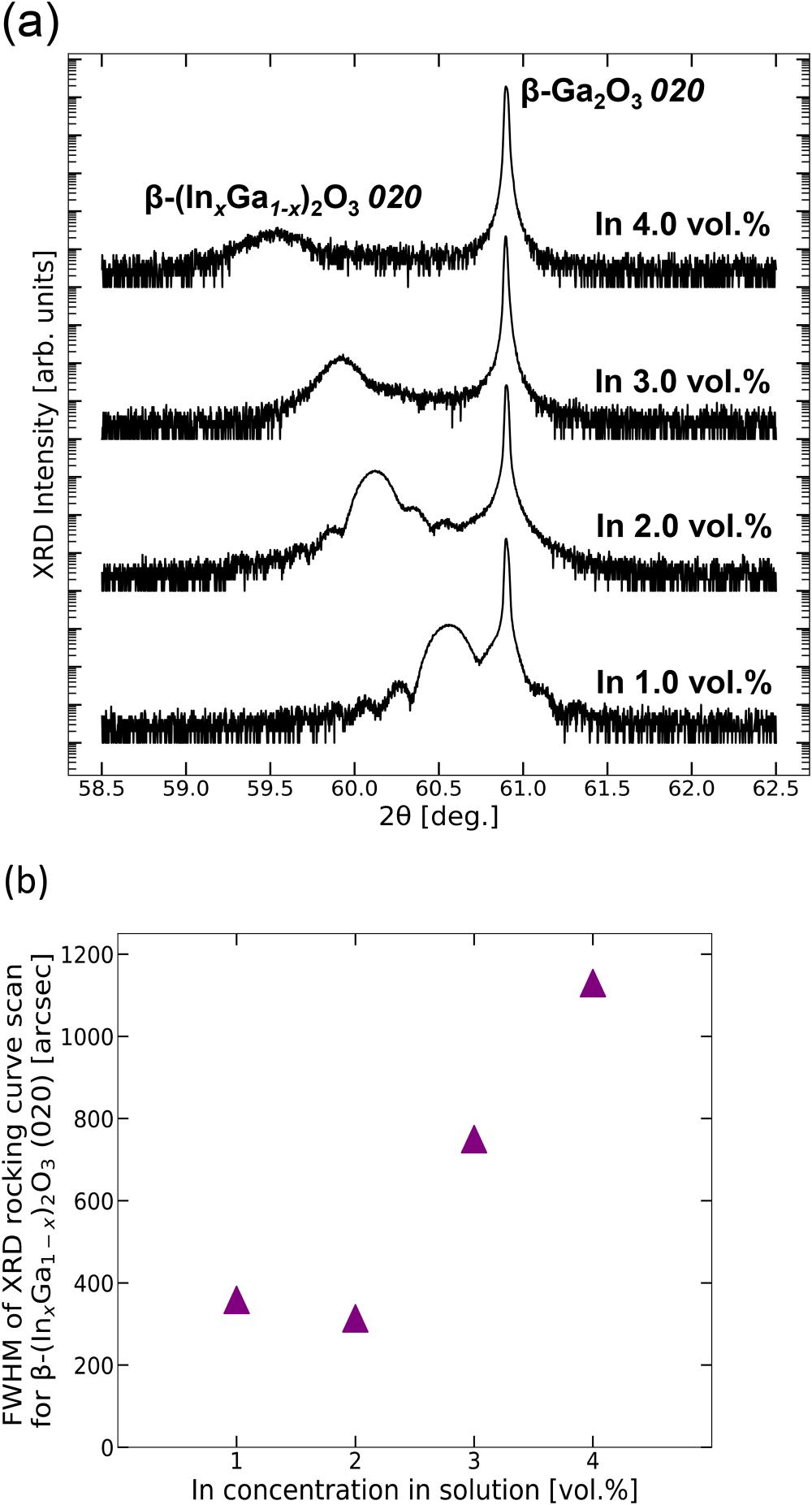
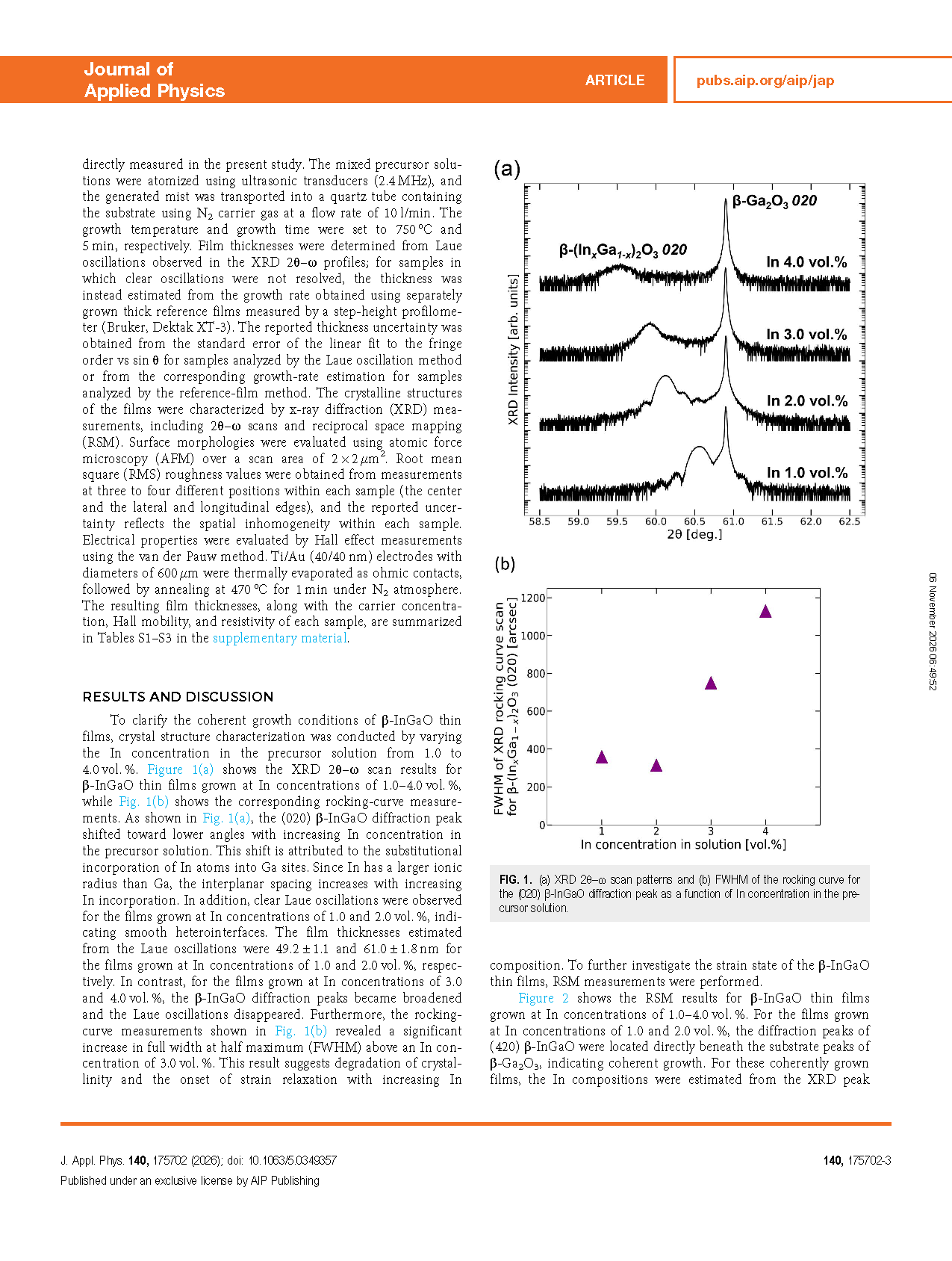
FIG. 1. (a) XRD 2θ–ω scan patterns and (b) FWHM of the rocking curve for the (020) β‑InGaO diffraction peak as a function of In concentration in the precursor solution.
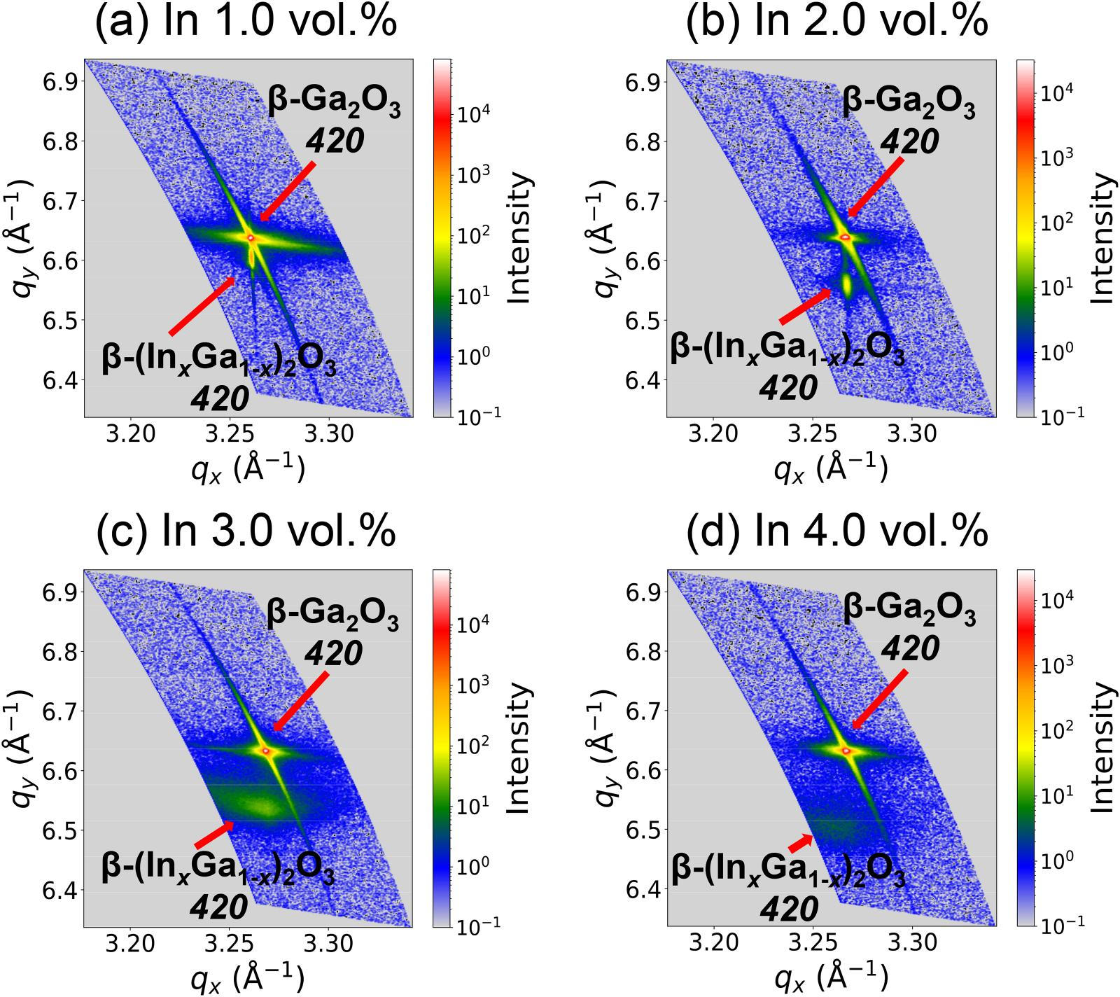
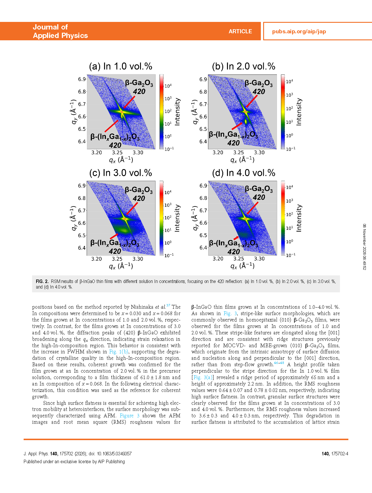
FIG. 2. RSM results of β‑InGaO thin films with different solution In concentrations, focusing on the 420 reflection: (a) In 1.0 vol. %, (b) In 2.0 vol. %, (c) In 3.0 vol. %, and (d) In 4.0 vol. %.
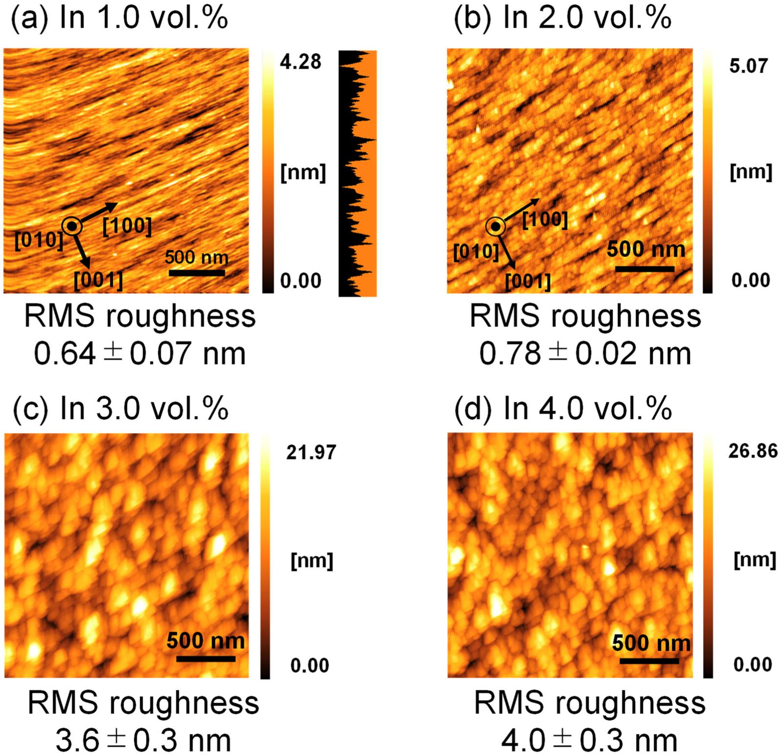
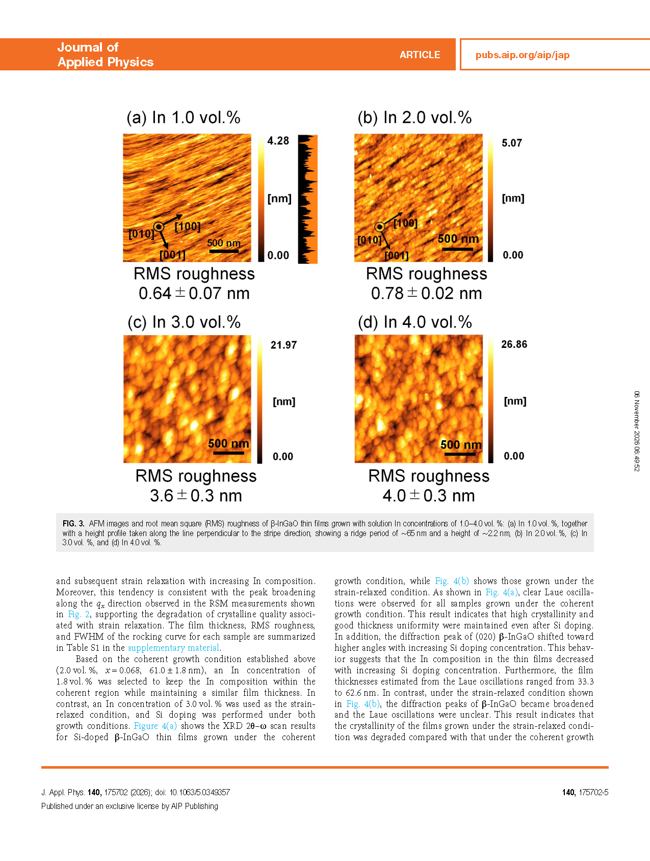
FIG. 3. AFM images and root mean square (RMS) roughness of β‑InGaO thin films grown with solution In concentrations of 1.0–4.0 vol. %: (a) In 1.0 vol. %, together with a height profile taken along the line perpendicular to the stripe direction, showing a ridge period of ∼65 nm and a height of ∼2.2 nm, (b) In 2.0 vol. %, (c) In 3.0 vol. %, and (d) In 4.0 vol. %.
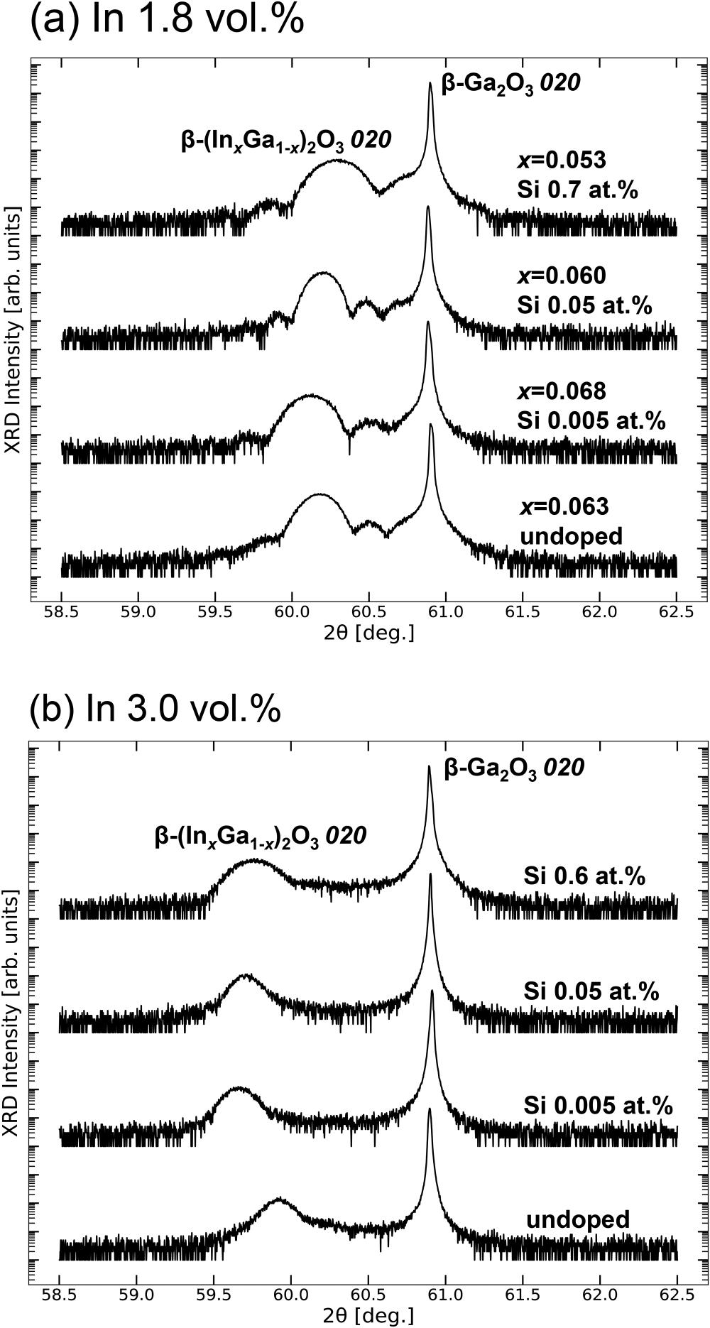
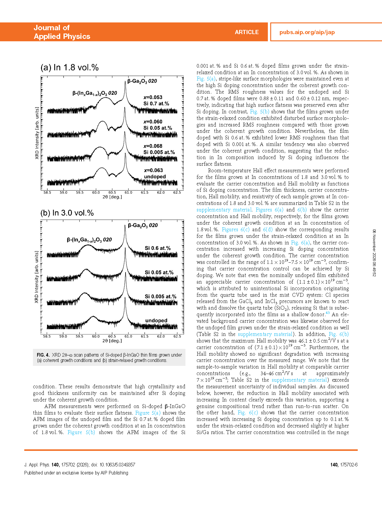
FIG. 4. XRD 2θ–ω scan patterns of Si‑doped β‑InGaO thin films grown under (a) coherent growth conditions and (b) strain‑relaxed growth conditions.
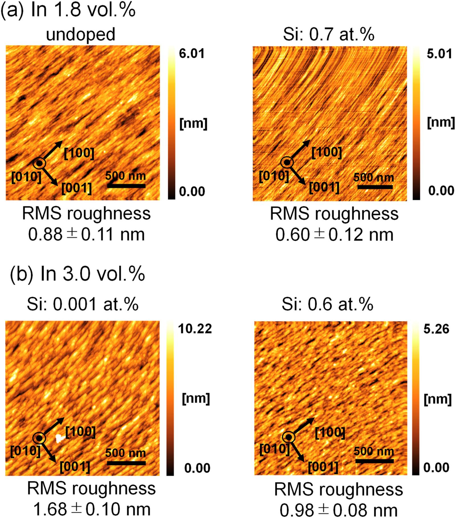
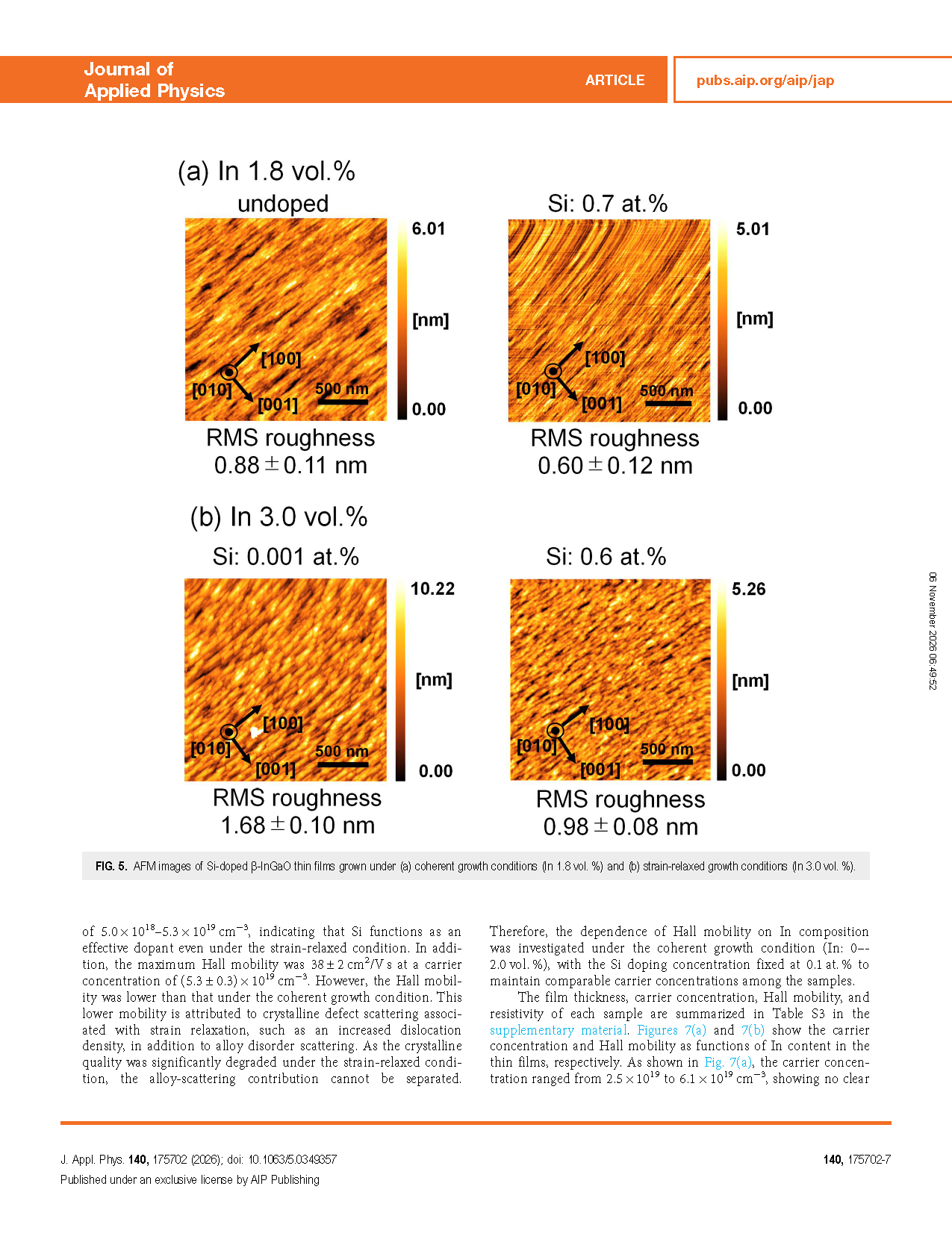
FIG. 5. AFM images of Si‑doped β‑InGaO thin films grown under (a) coherent growth conditions (In 1.8 vol. %) and (b) strain‑relaxed growth conditions (In 3.0 vol. %).
DOI:
doi.org/10.1063/5.0349357
Instruction
Official Account

Cooperation
Top
