


The Nanofabrication Facility of the Suzhou Institute of Nano-Tech and Nano-Bionics, Chinese Academy of Sciences, in collaboration with the University of Science and Technology of China, published a research paper entitled “Electro-optically co-modulated β-Ga₂O₃ floating-gate transistors for neuromorphic computing” in the international academic journal Science China Information Sciences. By combining the intrinsic solar-blind ultraviolet photoresponse of Ga₂O₃ with the nonvolatile charge-storage capability of floating-gate transistors, this study developed an electro-optically co-modulated multilevel conductance programming strategy, achieving microsecond-scale rapid write/erase operations and stable multilevel storage while demonstrating its potential for neuromorphic image recognition. Tiwei Chen is the first author, and Xiaodong Zhang and Baoshun Zhang are the corresponding authors. The paper was published online on October 28, 2026.
Background
As artificial intelligence advances toward edge sensing and real-time information processing, the data transfer latency and high energy consumption arising from the separation of memory and computing units in conventional von Neumann architectures have become increasingly prominent. Neural networks based on floating-gate transistors enable nonvolatile, multilevel programmable weight modulation through charge storage and release, providing a promising approach to developing neuromorphic computing systems with integrated memory and computation. Furthermore, introducing optical stimuli offers an additional dimension for synaptic weight modulation, with the potential to reduce programming energy consumption, improve interference immunity, and facilitate the integration of optical sensing and neuromorphic computing.
Gallium oxide (Ga₂O₃), with an ultra-wide bandgap of approximately 4.8 eV, exhibits an intrinsic solar-blind ultraviolet photoresponse that effectively suppresses interference from visible-light backgrounds, making it particularly attractive for optoelectronic neuromorphic devices. Currently, synaptic behaviors in Ga₂O₃-based neuromorphic devices are primarily achieved through carrier trapping and detrapping at deep-level defects. However, the formation and distribution of these defects are difficult to precisely control, often resulting in limited conductance programming accuracy, pronounced persistent photoconductivity, and slow programming speeds. These limitations hinder fast, stable, and reproducible synaptic weight updates. To address these challenges, the research team proposed a device architecture that spatially separates the optical absorption channel from the floating-gate charge storage structure. By combining capacitive coupling engineering with electro-optical co-programming, precise control over the conductance states of Ga₂O₃ floating-gate transistors was achieved, providing a new approach to the development of high-performance optoelectronic neuromorphic devices.
Abstract
To address the challenges associated with conventional Ga₂O₃-based synaptic devices, which rely on deep-level defects for conductance modulation and suffer from difficulties in precisely controlling defect states and pronounced persistent photoconductivity, the research team proposed a Ga₂O₃ floating-gate transistor architecture with spatially separated sensing and storage functions. The Ga₂O₃ channel enables solar-blind ultraviolet sensing, while the floating-gate structure provides nonvolatile conductance modulation through charge storage. Three complementary conductance programming strategies were further developed, including capacitive coupling modulation, electrical programming, and optical programming. By engineering the control-gate geometry, adjusting the programming voltage, and modulating ultraviolet illumination intensity, precise control over the memory window and synaptic conductance states was achieved.
Experimental results demonstrate that, through capacitive coupling modulation and electro-optical co-modulation, the device achieves a maximum memory window of 10 V, write and erase times as short as 120 μs, and stable 3-bit multilevel storage, while maintaining good reproducibility over 1000 consecutive write/erase cycles. Furthermore, leveraging the optoelectronic synaptic characteristics of the device, an artificial neural network was evaluated for handwritten digit recognition, achieving a maximum recognition accuracy of 96.0% under different ultraviolet illumination intensities. By spatially separating the sensing and storage functions, this study combines the intrinsic solar-blind ultraviolet photoresponse of Ga₂O₃ with the floating-gate charge storage mechanism, providing a promising approach to fast and precise synaptic weight modulation and the development of neuromorphic vision devices integrating sensing, memory, and computing.
Highlights
A separated optical-absorption and charge-storage architecture. The Ga₂O₃ channel performs solar-blind UV absorption, while the Ni floating gate and HfO₂ tunneling barrier provide charge storage.
Capacitive, electrical, and optical programming. Gate geometry, programming bias, and 254-nm illumination jointly tune the memory window up to 10 V.
Microsecond-scale multilevel storage. Eight resolved states support 3-bit operation, with 120-μs write/erase and 1,000 cycling tests.
Optically tunable neuromorphic recognition. Measured synaptic updates were incorporated into neural-network simulations for handwritten-digit recognition at different UV intensities.
Conclusion
By developing Ga₂O₃ floating-gate transistors with spatially separated sensing and storage functions, this study overcomes the limitations of conventional defect-dominated Ga₂O₃ synaptic devices in precise conductance modulation and enables multidimensional synaptic weight programming through capacitive coupling, electrical, and optical modulation. The devices exhibit microsecond-scale rapid write/erase operations, stable multilevel storage, and optoelectronic synaptic modulation capabilities, while demonstrating promising computational performance in neural network-based handwritten digit recognition. By combining the intrinsic solar-blind ultraviolet sensing capability of Ga₂O₃ with nonvolatile floating-gate charge storage, this work provides a new approach to the device-level integration of optical sensing, information storage, and neuromorphic computing, offering significant potential for advancing Ga₂O₃-based optoelectronic synaptic devices toward applications in intelligent ultraviolet vision, edge sensing, and integrated sensing-memory-computing systems.
Project Support
This work was supported in part by the Basic Research Program of Jiangsu (Grant No. BK20253003) and the Suzhou Critical Core Technology Research Project (Grant No. SYG2024003). The authors thank the Nano Fabrication Facility and Vacuum Interconnected Nanotech Workstation (NANO-X) of the Suzhou Institute of Nano-Tech and Nano-Bionics, Chinese Academy of Sciences, for technical support.
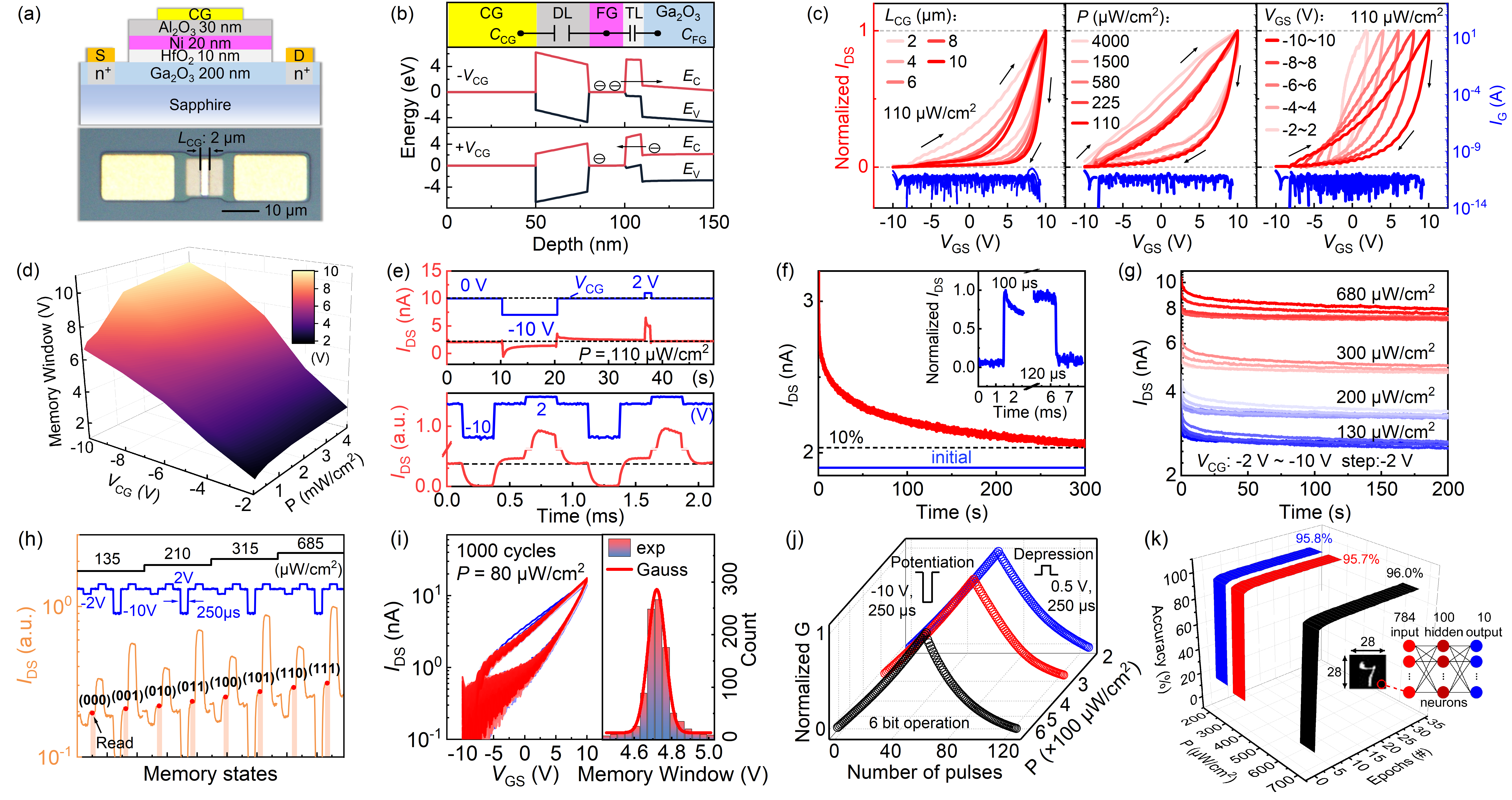
Figure 1 (a) Schematic and optical microscope images of the Ga₂O₃ FGT; (b) band structure of the Ga₂O₃ FGT; (c) transfer curves under different LCG, optical intensities, and VCG; (d) memory window as a function of optical intensity and VCG; (e) write and erase operations of the FGT; (f) retention characteristics of the FGT; (g) 20 states with each sampled for 200 s; (h) 3-bit multilevel storage of the FGT; (i) transfer curves from 1000 consecutive cycles; (j) potentiation and depression behaviors of the FGT under illumination with different intensities; (k) recognition rate as a function of the number of training epochs.
Research Team Introduction
The Ultra-wide Bandgap Semiconductor Research Team at the Suzhou Institute of Nano-Tech and Nano-Bionics, Chinese Academy of Sciences, has long been engaged in research on Group III oxide and nitride semiconductor materials and devices, with a focus on semiconductor film epitaxial growth, defect and interface engineering, optoelectronic device design, and micro/nanofabrication processes. The team has accumulated extensive research experience in high-quality Ga₂O₃ thin-film epitaxy, solar-blind ultraviolet photodetection, heterostructure design, and emerging optoelectronic devices, providing a solid foundation for the structural design, electro-optical co-modulation, and neuromorphic computing applications of Ga₂O₃ floating-gate transistors.
The team conducts its research with the support of the Nanofabrication Facility and the Vacuum Interconnected Nanotech Workstation (Nano-X) at SINANO. The Nanofabrication Facility features approximately 12,000 m2 of cleanroom space and more than 300 sets of equipment for micro/nanofabrication, testing, and packaging, providing comprehensive technical capabilities spanning semiconductor material growth, device fabrication, and performance characterization. In recent years, the team has undertaken multiple national, provincial, and municipal research projects and has achieved a series of research results in novel semiconductor materials and devices and chip integration, providing a research foundation and technical support for the development of ultra-wide bandgap semiconductor technology.
Author Profiles
Tiwei Chen received his Ph.D. degree from the University of Science and Technology of China and is currently a postdoctoral researcher at the Suzhou Institute of Nano-Tech and Nano-Bionics, Chinese Academy of Sciences. His research focuses on the epitaxial growth of ultra-wide-bandgap Ga₂O₃ semiconductors, optoelectronic device design, and integration technologies. He has made a series of research advances in high-quality heteroepitaxial thin films and high-speed, highly sensitive ultraviolet photodetectors, including the demonstration of Ga₂O₃ photodetector arrays integrated with readout circuits for real-time imaging. He has published six SCI-indexed papers as the first author in international journals, including Optics Letters, Journal of Materials Science & Technology. He holds three granted invention patents and has received several academic honors, including the Third Prize in the National Finals of the China Graduate IC Innovation Competition and a national-level scholarship.
DOI:
doi.org/10.1007/s11432-026-4912-4
Instruction
Official Account

Cooperation
Top
