


Researchers from the Xidian University and China Resources Microelectronics Limited have published a dissertation titled "Ultrathin Interlayer Engineered β-Ga₂O₃ Hybrid Schottky-Junction Rectifiers for High-Power Hard-Switching Conversion" in IEEE Transactions on Power Electronics.
Background
Power diodes are indispensable components in power electronic converters, where they are used for rectification, freewheeling, clamping, and protection. For high-voltage and high-power applications, a power diode must not only block high voltages and conduct large currents under static conditions, but also turn off safely and efficiently during hard commutation. Therefore, modern converters demand multiple simultaneous requirements, including low VF, low Ron,sp, high BV, surge-current ruggedness, low Qrr, soft recovery behavior, and converter-level high efficiency. The ultrawide-bandgap semiconductor β-Ga2O3 has emerged as a promising material platform for next-generation power rectifiers owing to its wide bandgap of approximately 4.8 eV, high predicted critical electric field, and availability of melt-grown substrates. Considerable progresses have been made in β-Ga2O3 diodes, ranging from high-voltage small-area devices for approaching material limits to large-area devices for practical current handling. Large-area Schottky barrier diodes (SBDs) offer low Von and majority-carrier switching, whereas heterojunction (HJ) PN diodes provide stronger electrostatic blocking capability and improved high-voltage margins. However, these device categories generally emphasize different aspects of power conversion: SBDs favor fast recovery and low conduction loss, while junction-based diodes favor high blocking capability but may introduce additional stored charge and recovery loss. A device concept that can bridge these two operating regimes is therefore needed for high-voltage hard-switching converters.
Abstract
Large-area β-Ga2O3 rectifiers have made substantial progress in static voltage blocking and current handling; however, converter applications also require controlled reverse recovery, surge-current ruggedness, and low-loss hard commutation. This paper investigates an ultrathin p-Cr2O3 interlayer design for vertical β-Ga2O3 rectifiers, in which the interlayer thickness tunes the anode transport from Schottky-dominated conduction toward junction-influenced operation. A series of devices with 0-, 5-, 10-, 15-, and 20-nm p-Cr2O3 interlayers shows that the 5-nm device operates in a hybrid Schottky–junction (HSJ) regime, improving reverse blocking while preserving low-voltage conduction. A 9 mm2 and 5-nm p-Cr2O3/β-Ga2O3 diode with ion-implanted edge termination (ET) exhibits a turn-on voltage (Von) near 1 V, a specific on-resistance (Ron,sp) of 8-9 mΩ·cm2, and a breakdown voltage (BV) of approximately 1.8 kV. After packaging, the diode conducts 60 A at a forward voltage (VF) of 10 V and withstands a 40 A surge current with 1.60-J absorbed energy. Under 30 A/400 V hard commutation, it shows a peak reverse-recovery current (IRRM) of 1.48 A, reverse-recovery time (trr) of 31.3 ns, reverse recovery charge (Qrr) of 30.1 nC, and a softness factor of 3.44. Implemented in a boost converter, the diode delivers approximately 1.45 kW output power (Pout) with 98.6% efficiency.
Highlights
The introduction of a 5 nm p-Cr₂O₃intermediate layer on the β-Ga₂O₃anode side forms a hybrid Schottky junction (HSJ) rectifier, achieving a balance between a low forward conduction voltage and a high reverse blocking capability.
Following ion implantation of the edge terminals, the 9 mm² device exhibits an on-voltage of approximately 1 V, a specific on-resistance of 8–9 mΩ·cm², and a breakdown voltage of approximately 1.8 kV.
The packaged device can conduct 60 A at a forward voltage of 10 V and withstand a surge current of 40 A, absorbing 1.60 J of energy.
Under hard-switching conditions of 30 A/400 V, the reverse recovery time is 31.3 ns, the reverse recovery charge is 30.1 nC, the peak reverse recovery current is 1.48 A, and the softness factor is 3.44.
In a boost converter, an output power of approximately 1.45 kW and a conversion efficiency of 98.6 per cent were achieved, demonstrating the device’s potential for application in high-power hard-switching power electronic systems.
Conclusion
This paper demonstrates an ultrathin p-Cr2O3 interlayer approach for large-area β-Ga2O3 hybrid rectifiers. By comparing devices with 0-, 5-, 10-, 15-, and 20-nm p-Cr2O3 interlayers, the static characteristics reveal a thickness-dependent transition from Schottky-dominated behavior toward more junction-influenced operation. Among these designs, the 5-nm interlayer provides a balanced hybrid operating point that preserves low-voltage forward conduction while improving reverse-blocking capability. The large-area 9-mm2 5-nm p-Cr2O3/β-Ga2O3 HSJ diode with ion-implanted ET achieves a Von of approximately 1 V, a Ron,sp of 8-9 mΩ·cm2, and a BV of approximately 1.8 kV. After packaging, the device conducts up to 60 A and sustains a 40-A surge-current pulse with an extracted surge energy of 1.60 J. Under 30 A/400 V hard commutation, the packaged diode maintains a low IRRM of 1.48 A, a trr of 31.3 ns, a Qrr of 30.1 nC, and a softness factor S of 3.44. In boost-converter operation, the diode enables a Pout of approximately 1.45 kW with a calculated efficiency of 98.6%. These results indicate that ultrathin-interlayer engineering provides an effective route for balancing static blocking, high-current capability, and hard-commutation recovery behavior in large-area β-Ga2O3 rectifiers. The key design implication is that the interlayer should be sufficiently effective in enhancing blocking capability while remaining thin enough to avoid excessive VF penalty and charge-storage effects associated with strongly junction-dominated operation.
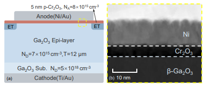
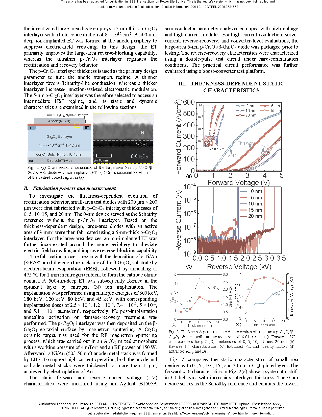
Fig. 1. (a) Cross-sectional schematic of the large-area 5-nm p-Cr2O3/β-Ga2O3 HSJ diode with ion-implanted ET. (b) Cross-sectional SEM image of the dashed-boxed region in (a).
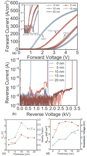
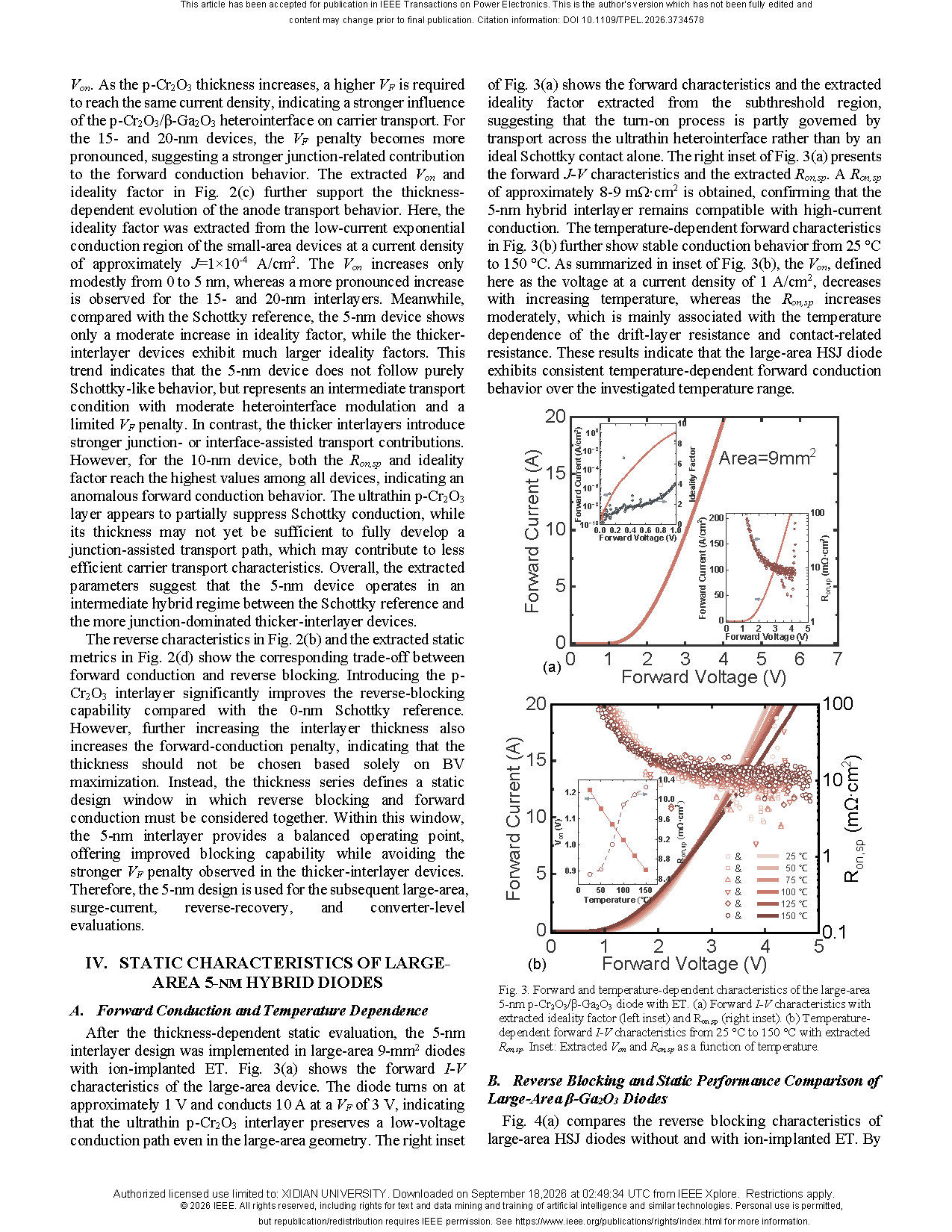
Fig. 2. Thickness-dependent static characteristics of small-area p-Cr2O3/β-Ga2O3 diodes with an active area of 0.04 mm2. (a) Forward J-V characteristics for p-Cr2O3 thicknesses of 0, 5, 10, 15, and 20 nm. (b) Reverse I-V characteristics. (c) Extracted Von and ideality factor. (d) Extracted Ron,sp and BV.
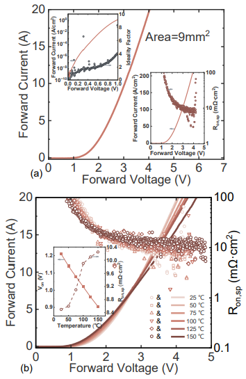
Fig. 3. Forward and temperature-dependent characteristics of the large-area 5-nm p-Cr2O3/β-Ga2O3 diode with ET. (a) Forward I-V characteristics with extracted ideality factor (left inset) and Ron,sp (right inset). (b) Temperature-dependent forward I-V characteristics from 25 °C to 150 °C with extracted Ron,sp. Inset: Extracted Von and Ron,sp as a function of temperature.
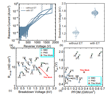
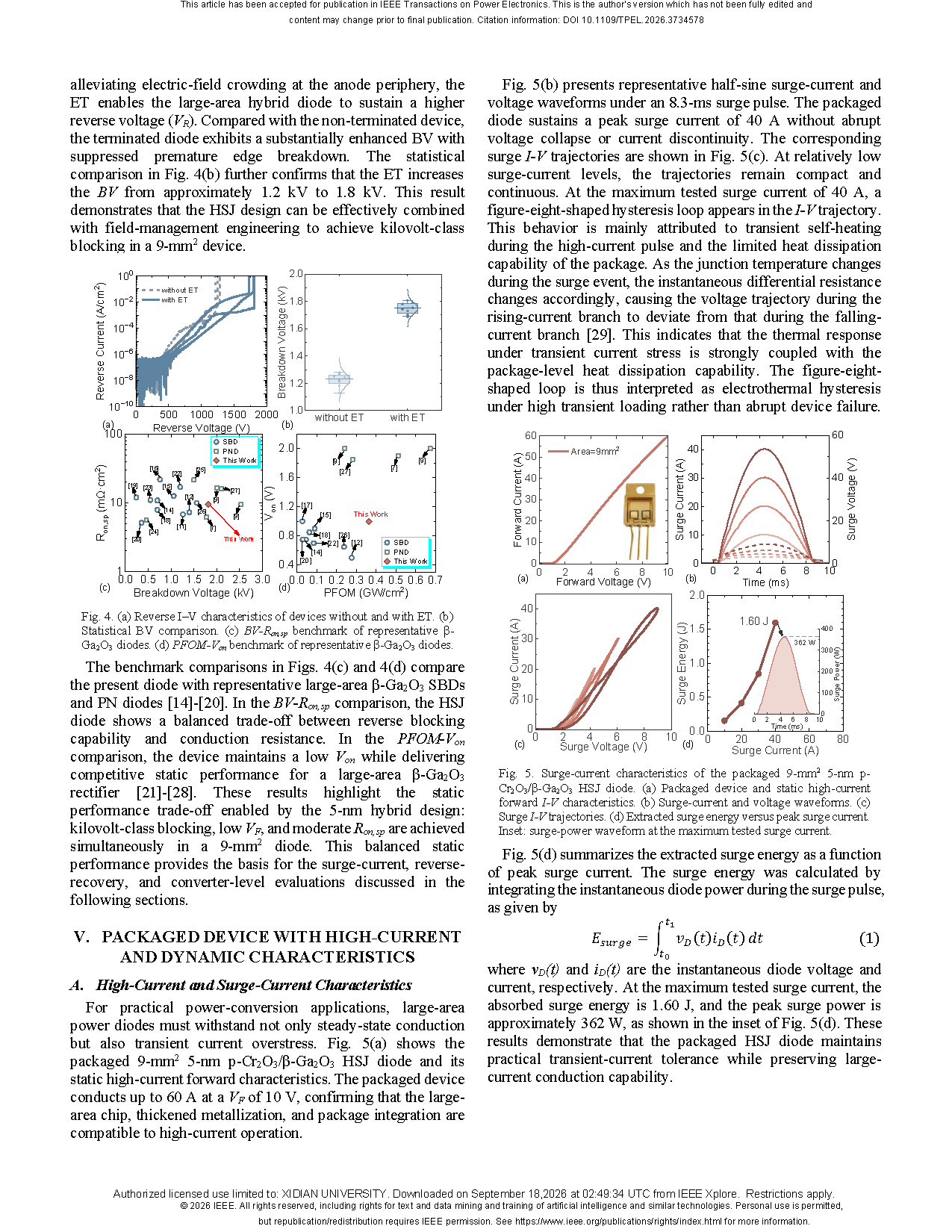
Fig. 4. (a) Reverse I–V characteristics of devices without and with ET. (b) Statistical BV comparison. (c) BV-Ron,sp benchmark of representative β-Ga2O3 diodes. (d) PFOM-Von benchmark of representative β-Ga2O3 diodes.
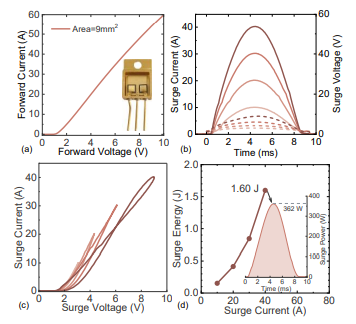
Fig. 5. Surge-current characteristics of the packaged 9-mm2 5-nm p-Cr2O3/β-Ga2O3 HSJ diode. (a) Packaged device and static high-current forward I-V characteristics. (b) Surge-current and voltage waveforms. (c) Surge I-V trajectories. (d) Extracted surge energy versus peak surge current. Inset: surge-power waveform at the maximum tested surge current.
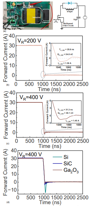
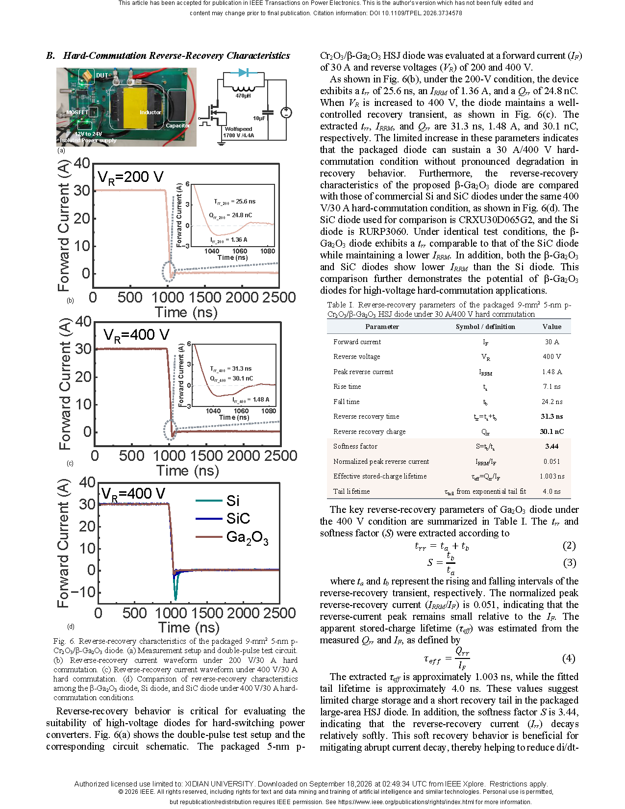
Fig. 6. Reverse-recovery characteristics of the packaged 9-mm2 5-nm p-Cr2O3/β-Ga2O3 diode. (a) Measurement setup and double-pulse test circuit. (b) Reverse-recovery current waveform under 200 V/30 A hard commutation. (c) Reverse-recovery current waveform under 400 V/30 A hard commutation. (d) Comparison of reverse-recovery characteristics among the β-Ga2O3 diode, Si diode, and SiC diode under 400 V/30 A hard-commutation conditions.
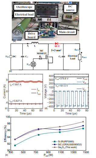
Fig. 7. Boost-converter evaluation of the packaged 9-mm2 5-nm p-Cr₂O₃/β-Ga₂O₃ HSJ diode. (a) Experimental setup. (b) Boost-converter test circuit. (c) Measured Iin and Iout. (d) Measured Vin, Vout and Vd. (e) Comparison of conversion efficiencies of the proposed β-Ga2O3 diode and commercial Si and SiC diodes.
DOI:
doi.org/10.1109/TPEL.2026.3734578
Instruction
Official Account

Cooperation
Top
