


Gallium oxide (Ga₂O₃) has a theoretical critical breakdown field strength of approximately 8 MV/cm, making it a promising candidate material for high-voltage power electronic devices. However, its material advantages do not automatically translate into stable device operation. Under sustained bias, elevated temperatures, and repeated electrical stress, charge trapping and detrapping at defect sites may alter carrier transport and the electric field distribution within devices, leading to variations in key parameters such as on-state conduction and breakdown voltage.
To address the operational stability challenges of Ga₂O₃ devices, the Han-NVM research group at Xidian University has focused on controlling charges associated with intrinsic defects in Ga₂O₃. On one hand, holes supplied by the p-NiO side are used to compensate for negative charges near the interface within the Ga₂O₃ bulk, improving the conduction characteristics of bipolar diodes. On the other hand, by regulating the spatial distribution of localized defect charges, the team has sought to reshape the electric field distribution at the anode edge of unipolar devices, exploring a pathway toward enhanced breakdown voltage.
These studies demonstrate the role of intrinsic defect engineering in optimizing Ga₂O₃ device performance from two complementary perspectives: the regulation of defect charge states and the control of their spatial distribution.
Intrinsic Defect Charge Engineering: Improving On-State Conduction and Breakdown Performance
Intrinsic defects in Ga₂O₃, including gallium vacancies (VGa), oxygen vacancies (VO), and their complexes, can trap or release charges under the influence of electric fields and temperature, thereby affecting carrier transport and the internal electric field distribution of devices. Although defect-related charges are commonly associated with performance degradation, their effects are not necessarily detrimental. Studies have shown that, under specific bias conditions, regulating the charge states or spatial distribution of defects may also help improve device conduction and blocking performance.
1.Charge-State Regulation: Near-Interface Charge Compensation in Ga₂O₃ Improves Bipolar Device Conduction
During stepped forward-bias stress testing of p-NiO/n-Ga₂O₃ heterojunction diodes, the specific on-resistance initially decreased from approximately 2.7 mΩ·cm² to 1.8 mΩ·cm² as the stress voltage increased, before rising to approximately 3.4 mΩ·cm² under stronger electrical stress.
The study suggests that holes injected during the 4–6 V stress stage participate in filling near-interface traps and regulating charges within the Ga₂O₃ bulk, helping to reduce the on-resistance. When the voltage increases to 7–8 V, however, self-heating induced by the high current begins to affect carrier transport. At 7 V, the device junction temperature reaches approximately 140 °C.
Meanwhile, negative space charges associated with gallium vacancies may accumulate near the heterojunction interface, producing electrostatic screening that hinders hole injection.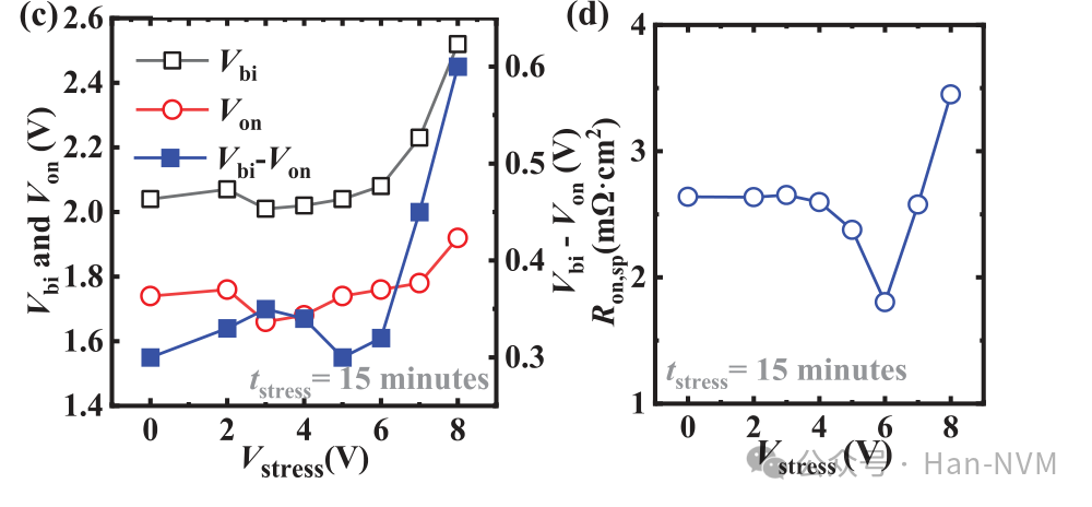
Figure 1 | Specific on-resistance initially decreases and then increases with increasing forward stress voltage under stepped forward-bias stress. Original figure from IEEE Transactions on Electron Devices, 72(11), 5906–5912 (2025). DOI: 10.1109/TED.2025.3610332.
With the forward voltage further fixed at 8 V, the device on-state current initially decreases and then recovers over the course of the stress test. The study divides this process into two stages. During the CT-I stage, deep-level defects associated with gallium vacancies trap electrons, leading to an accumulation of negative space charge near the interface within the Ga₂O₃ bulk and hindering carrier transport. During the CT-II stage, holes injected from the NiO side gradually compensate for the negative charges accumulated during the preceding stage. Consequently, the on-state current recovers and the specific on-resistance decreases, while the turn-on voltage and forward voltage drop also improve. The ideality factor is reduced to approximately 1.03.
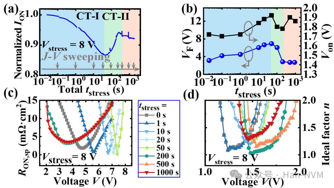
Figure 2 | Under a constant 8 V forward-bias stress, the on-state current initially decreases and then recovers, indicating an improvement in device conduction performance over time. Original figure from IEEE Transactions on Electron Devices, 72(10), 6345–6348 (2026). DOI: 10.1109/TED.2026.3723573.
To identify where charge compensation occurs, the study combined transport analysis, temperature-dependent kinetic measurements, dynamic secondary ion mass spectrometry (D-SIMS), and C–V depth profiling. The results show that the major charge variations are concentrated within a region approximately 100 nm from the interface on the Ga₂O₃ side. During the CT-II stage, the heterojunction diodes incorporating NiO exhibit more complete near-interface charge recovery, whereas Schottky diodes without NiO show only partial recovery. This comparison supports the interpretation that holes injected from the NiO side participate in compensating the negative charges.
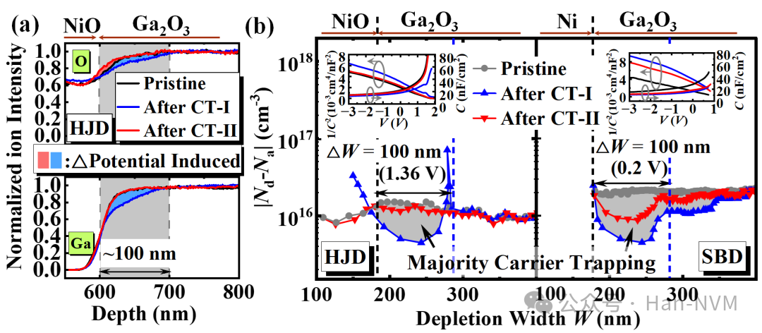
Figure 3 | Charge variations are primarily concentrated within approximately 100 nm of the interface on the Ga₂O₃ side, with devices incorporating NiO exhibiting more complete charge compensation. Original figure from IEEE Transactions on Electron Devices, 72(10), 6345–6348 (2026). DOI: 10.1109/TED.2026.3723573.
Reliability testing further shows that, following charge regulation under an 8 V stress for 1,000 s, the devices maintain relatively stable parameters during a subsequent 10,000 s retention test. The average breakdown voltage also recovers from 875 V after degradation in the CT-I stage to 938 V. These results indicate that the effects of defect-related charges on device performance evolve with stress conditions and time, and that initial performance degradation does not necessarily reflect the device's long-term state.
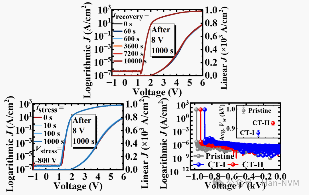
Figure 4 | Following charge regulation, the devices maintain favorable on-state conduction and breakdown characteristics during long-term retention and reverse-bias stress testing. Original figure from IEEE Transactions on Electron Devices, 72(10), 6345–6348 (2026). DOI: 10.1109/TED.2026.3723573.
2.Spatial Distribution Engineering of Defect Charges: Localized Negative Charges Form a “Virtual Field Plate”
For unipolar devices, the research group further investigated the spatial distribution of intrinsic defect charges. In Ga₂O₃-on-SiC transistors, sustained positive gate-bias stress causes the threshold voltage to first shift positively and then negatively, while the on-resistance decreases with stress time.
The study suggests that negatively charged gallium vacancies can electrostatically attract hydrogen ions (H⁺). The accumulated hydrogen passivates deep acceptor states associated with gallium vacancies and forms complex defects with shallow donor characteristics, thereby increasing the free-electron concentration in the channel.
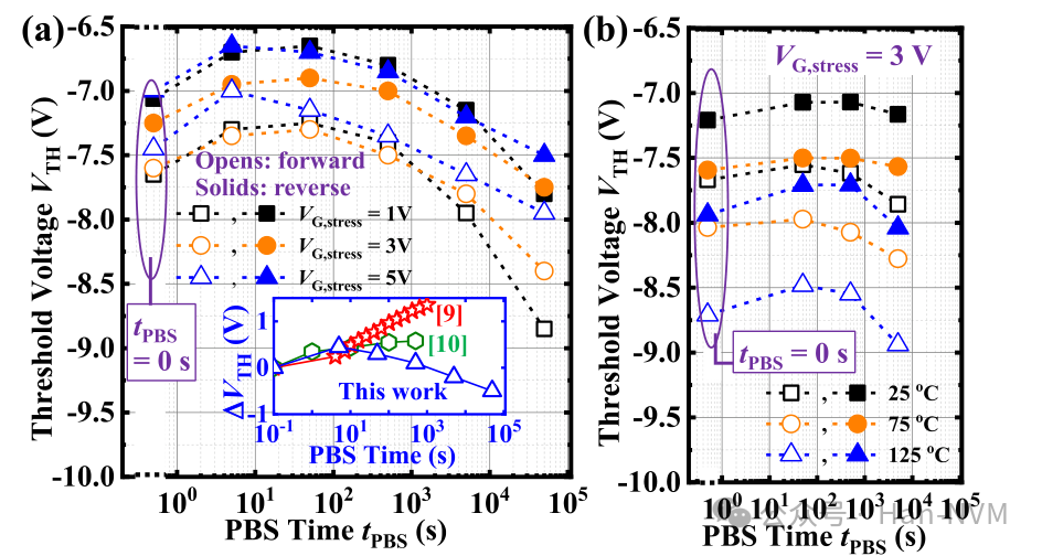
Figure 5 | Under sustained bias stress, the threshold voltage of Ga₂O₃-on-SiC transistors initially shifts in the positive direction and then shifts in the negative direction. Original figure from IEEE Electron Device Letters, 44(8), 1256–1259 (2023). DOI: 10.1109/LED.2023.3288820.
Building on this work, the study further examined reverse-blocking conditions to determine whether localized negative charges could redistribute the electric field and alleviate the local field concentration at the electrode edge. TCAD simulations show that, under controlled negative-bias conditions, VGa–VO complex defects near the anode edge can trap electrons, forming localized negative space charges.
The simulation results indicate that these charges can reshape the potential distribution at the edge, causing the depletion region to extend laterally along the interface and reducing the local peak electric field. This produces an equivalent field-plate effect without the need for additional metal field-plate structures, known as the “Virtual Field Plate” effect.
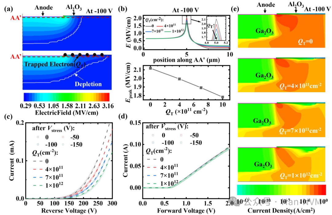
Figure 6 | TCAD simulations reveal the “Virtual Field Plate” effect of localized negative charges. (a) Electric-field distribution and depletion-region evolution near the anode edge; (b) increased localized negative charge density reduces the peak electric field; (c–d) reverse leakage is suppressed while forward conduction characteristics remain largely unchanged; (e) suppression of the reverse leakage path near the anode edge. Original figure from Applied Physics Letters, 129(11), 113505 (2026). DOI: 10.1063/5.0344318.
Device measurements are consistent with the proposed mechanism. Following controlled negative-bias stress at −250 V for 1,000 s, the average breakdown voltage of five devices increased from 306 V to 397 V, representing a 29.7% improvement. The reverse leakage current decreased by approximately 91%, while the forward conduction characteristics remained largely unchanged.
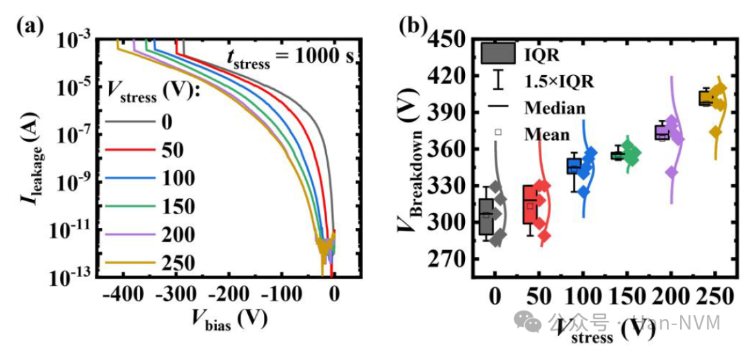
Figure 7 | Reverse I–V characteristics and breakdown voltage statistics of the devices before and after controlled stress. The average breakdown voltage increased from 306 V to 397 V, representing a 29.7% improvement. Original figure from Applied Physics Letters, 129(11), 113505 (2026). DOI: 10.1063/5.0344318.
The charge reconstruction also exhibits a degree of reversibility. After the stress was removed, the devices were left at room temperature for 1,000 s, during which the reverse leakage current increased only slightly. Following thermal treatment at 400 K for 1,000 s, electrons trapped at defect sites were gradually released, and the reverse leakage current largely returned to its initial level. The average breakdown voltage decreased from 397 V to 333 V, gradually approaching its initial value of 306 V. These results further support the conclusion that the improvement in breakdown voltage is associated with localized space-charge reconstruction rather than irreversible material damage.
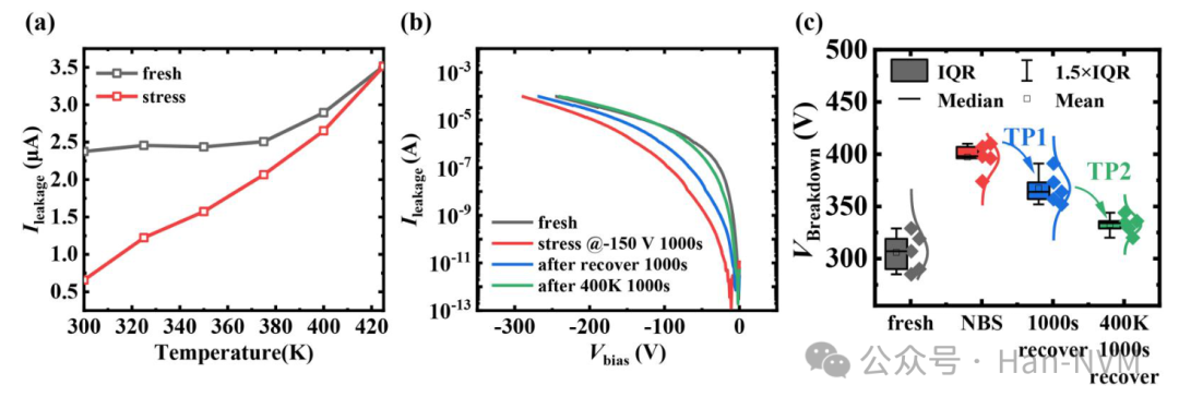
Figure 8 | Temperature-dependent and thermal recovery experiments: leakage suppression weakens with increasing temperature, and the reverse-bias characteristics recover after treatment at 400 K, with the breakdown voltage gain gradually diminishing. Original figure from Applied Physics Letters, 129(11), 113505 (2026), Fig. 5(a–c). DOI: 10.1063/5.0344318.
Intrinsic Defect Charge Engineering: Multidimensional Approaches to Ga₂O₃ Device Reliability
The studies discussed above demonstrate two approaches to improving the reliability of Ga₂O₃ devices. In both bipolar and unipolar devices, the research group focuses on the dynamic behavior of charges associated with intrinsic defects. In bipolar diodes, holes injected from the NiO side compensate for negative charges near the interface within the Ga₂O₃ bulk, improving on-state conduction. In unipolar devices, localized negative charges reshape the electric field near the anode edge, producing a “Virtual Field Plate” effect that enhances voltage-blocking capability.
These studies demonstrate how intrinsic defect engineering affects Ga₂O₃ device performance from two complementary perspectives: charge-state regulation and spatial charge distribution. In p-NiO/n-Ga₂O₃ bipolar diodes, holes injected from the NiO side compensate for negative space charges near the interface within the Ga₂O₃ bulk, allowing device conduction performance to recover and improve under electrical stress. In Ga₂O₃-on-SiC unipolar devices, localized negative charges reshape the electric field near the anode edge, producing a “Virtual Field Plate” effect and thereby improving reverse-blocking characteristics.
These findings suggest that intrinsic defects are not solely associated with device performance degradation. Their charge states, spatial distributions, and dynamic responses to bias and temperature may also be important factors to consider in device design and performance optimization.
From understanding the dynamic evolution of defect-related charges to exploring ways to actively regulate them, these studies offer new approaches to optimizing both on-state conduction and voltage-blocking performance in Ga₂O₃ power devices.
References
[1] C. Yu et al.,“Dynamics of Forward Bias-Induced On-State Parameter Shift in p-NiO/β-Ga2O3 Heterojunction Diodes,” IEEE Transactions on Electron Devices, vol. 72, no. 11, pp. 5906 - 5912, Nov. 2025. DOI: 10.1109/TED.2025.3610332.
[2] C. Yu et al., “Reliability Enhancement of Ga2O3 Heterojunction Diodes Due to Space-Charge Modulation,” IEEE Transactions on Electron Devices, vol. 73, no. 10, pp. 6345-6348, Oct. 2026. DOI: 10.1109/TED.2026.3723573.
[3] J. Liao et al., “Electric Field Reconfiguration in W/β-Ga2O3 Schottky Barrier Diodes under Negative Bias Stress,” Applied Physics Letters, vol.129, no. 11, Art. No. 113505, Sept. 2026. Doi: 10.1063/5.0344318.
[4] C. Yu et al., “Annealing-Driven Strain Relaxation Transition and Its Direct Impact on Transport in Heteroepitaxial β-Ga2O3 MOSFETs,” IEEE Transactions on Electron Devices, vol. 73, no. 8, pp. 5134 - 5139, Aug. 2026. DOI: 10.1109/TED.2026.3701688.
[5] C. Liu et al., “Unique Monotonic Positive Shifts in Threshold Voltages of Ga2O3-on-SiC MOSFETs Under Both Unipolar Positive and Negative Bias Stresses,” IEEE Transactions on Electron Devices, vol. 72, no. 3, pp. 1047-1052, March 2025. DOI: 10.1109/TED.2025.3534742.
[6] C. Liu et al., “Dynamic Performance Enhancement in Ti/Au Ohmic Contacts on β-Ga2O3-on-SiC Substrates: Evidence from Pulsed Measurements,” SCIENCE CHINA Information Sciences, vol. 68, no. 1, pp. 119403, Jan. 2025.
[7] C. Yu et al., “Enhancing β-Ga2O3 Schottky Barrier Diodes Performance through Low-Temperature Post Annealing: Achieving Optimal Forward Current-Voltage Characteristics,” IEEE Transactions on Electron Devices, vol.71, no. 9, pp. 5552-5558, Sept. 2024.
[8] C. Liu et al., “Unique Bias Stress Instability of Heterogeneous Ga2O3-on-SiC MOSFET,” IEEE Electron Device Letters, vol. 44, no. 8, pp. 1256-1259, Aug. 2023. DOI: 10.1109/LED.2023.3288820.
Instruction
Official Account

Cooperation
Top