


Researchers from North China University of Technology, Beijing University of Technology, Institute of Semiconductors, Chinese Academy of Sciences and other institutions have published a paper titled "A Solar‑Blind Photodetector Based on MXene/β‑Ga₂O₃ Heterojunction With Superlinear Photoresponse and Synaptic Plasticity" in Laser & Photonics Reviews.
Background
The demand for wide‑dynamic‑range photodetectors is pressing, yet conventional devices are restricted to fixed‑mode operation, where a single transport mechanism fundamentally limits the performance ceiling of individual photodetectors. Modern optoelectronic systems are rapidly evolving toward multifunctional, intelligent, and all‑weather operation, while practical environments are characterized by drastic illumination fluctuations and frequent switching between bright and dark states. Such demanding conditions urgently require photodetectors with light‑intensity‑dependent detection capability across the full optical power range. Under high‑intensity illumination, strong anti‑saturation capability is required to avoid optical overload and prevent photocurrent distortion. For low‑intensity illumination, high‑magnitude photoconductive gain mechanisms are essential to achieve high‑sensitivity detection and efficient weak‑signal collection. Nevertheless, it remains a formidable challenge to develop photodetectors capable of operating under both high‑intensity and low‑intensity illumination. The core reason lies in the fundamental trade‑off between the carrier dynamics required for superlinear operation under high‑intensity light and those required for high‑gain amplification under weak light.
β‑Ga₂O₃ an ultra‑wide bandgap semiconductor, exhibits excellent physical properties for high‑performance optoelectronic devices. Its ultra‑wide bandgap of ∼ 4.8 eV endows β‑Ga₂O₃‑based photodetectors with the ability to avoid dark‑current swamping, radiation‑induced degradation, and thermally induced linearization, thus making them promising for achieving high optical saturation thresholds and stable performance under high‑intensity operation. In addition, this semiconductor possesses abundant intrinsic defect energy levels with flexible tunability. Precise control over defect concentration and interfacial band bending allows the construction of carrier dynamics within devices. Trap‑mediated photoconductive gain supports signal amplification under weak light, while rapid carrier relaxation kinetics mitigate photocurrent saturation at high optical power. Benefiting from its distinctive electronic band structure, tunable defect‑state dynamics, and excellent operational stability, β‑Ga₂O₃ serves as a reliable multifunctional material platform for photodetectors with a broad dynamic range and light‑intensity‑dependent capability.
Abstract
The demand for wide‑dynamic‑range photodetectors is pressing, yet conventional devices are restricted to fixed‑mode operation, where a single transport mechanism fundamentally limits the performance ceiling of individual photodetectors. Here, we demonstrate a photodetector based on an MXene/β‑Ga₂O₃ van der Waals Schottky junction, whose operational characteristics are governed by the incident light intensity. This heterostructure enables efficient photocarrier separation and interfacial barrier modulation, allowing the device to exhibit distinct working behaviors under different illumination conditions at zero bias. Under strong deep‑ultraviolet irradiation, the device delivers a superlinear photoresponse with a power‑law exponent of 1.47, enabling high‑sensitivity detection of strong signals. By contrast, in the weak‑light regime, the device manifests typical synaptic plasticity features, including pronounced excitatory postsynaptic current, a paired‑pulse facilitation index of up to 200%, and a dynamic transition from short‑term plasticity to long‑term plasticity. This work provides a general pathway for constructing light‑triggered multifunctional optoelectronic devices via interfacial carrier dynamics control, thereby laying a foundation for the advancement of photodetection systems.
Highlights
An MXene/β‑Ga₂O₃ van der Waals Schottky‑junction photodetector is constructed. Without extra structural optimization, device working modes can be tuned by incident light intensity.
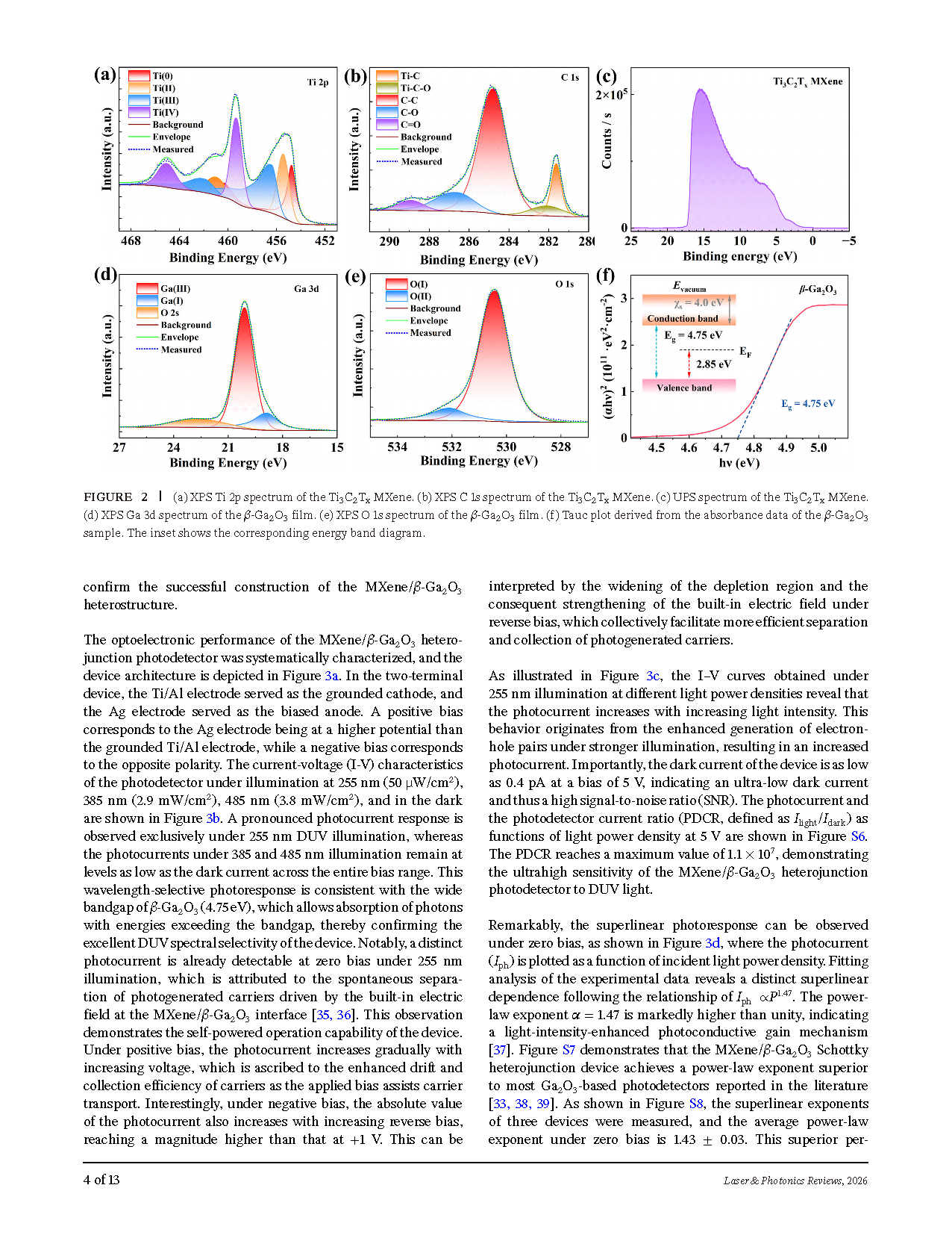
Superlinear photoresponse is achieved under zero‑bias strong deep‑ultraviolet illumination with maximum power‑law exponent of 1.47. The exponent keeps above unity under applied bias, greatly broadening dynamic range. At 5 V bias, the device achieves light‑dark current ratio of 1.1 ×10⁷, responsivity of 280 mA/W, specific detectivity of 2.1 ×10¹¹ Jones and external quantum efficiency up to 140 %.
Under weak‑light zero‑bias conditions, the device exhibits complete neuromorphic synaptic behaviors, including excitatory postsynaptic current, paired‑pulse facilitation (PPF index up to 200 %), and transition from short‑term to long‑term plasticity, which emulates biological learning and memory.
Dual‑mode physical mechanisms are clarified:Under strong illumination, photogenerated carriers fill the traps and induce trap saturation, giving rise to superlinear photoresponse; under weak illumination, the trapping–detrapping process modulates carrier transport to achieve synaptic plasticity.
The device supports self‑powered photodetection and reliably receives binary optical pulses for deep‑ultraviolet optical communication. It exhibits good ambient‑storage stability and cyclic operating stability, promising for low‑power neuromorphic vision and adaptive imaging applications.
Conclusion
In this work, an MXene/β‑Ga₂O₃ van der Waals heterojunction photodetector is constructed. The device exhibits distinct photoresponse behaviors under different illumination conditions. Under strong light illumination, it shows a superlinear photoresponse with power‑law fitting exponent α reaches 1.47 at 0 V and 1.70 at 4 V. This demonstrates that the device exhibits excellent optoelectronic modulation performance and operational stability over a wide bias range, enabling high‑sensitivity detection across broad light intensity ranges. Under weak light and zero‑bias conditions, the device efficiently emulates the core behaviors of biological synapses. The PPF index reaches 200%, consistent with the STP characteristics of biological synapses, highlighting the outstanding self‑powered synaptic performance. The proposed device achieves the synergistic integration of superlinear photoresponse and self‑powered synaptic functionality. It holds great promise for applications in emerging fields such as low‑power neuromorphic vision systems and intelligent ultraviolet perception.
Project Support
This work was supported by the Open Project Program of Shanxi Key Laboratory of Advanced Semiconductor Optoelectronic Devices and Integrated Systems (No. 2025SZKF08) and the Youth Research Special Project of NCUT (No. 110051360025XN077‑37).
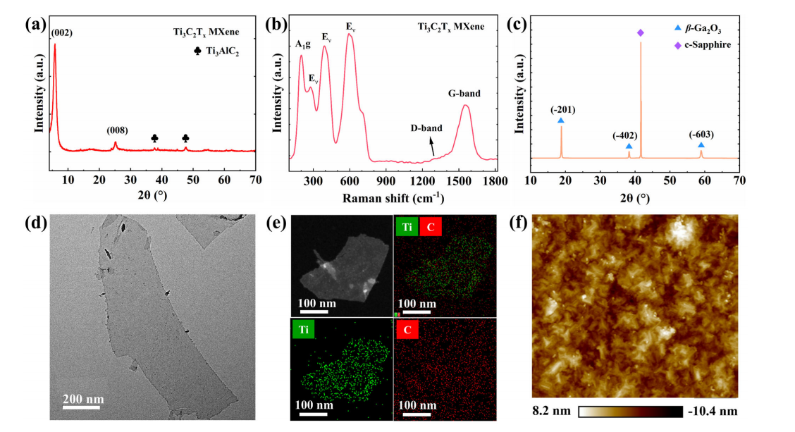
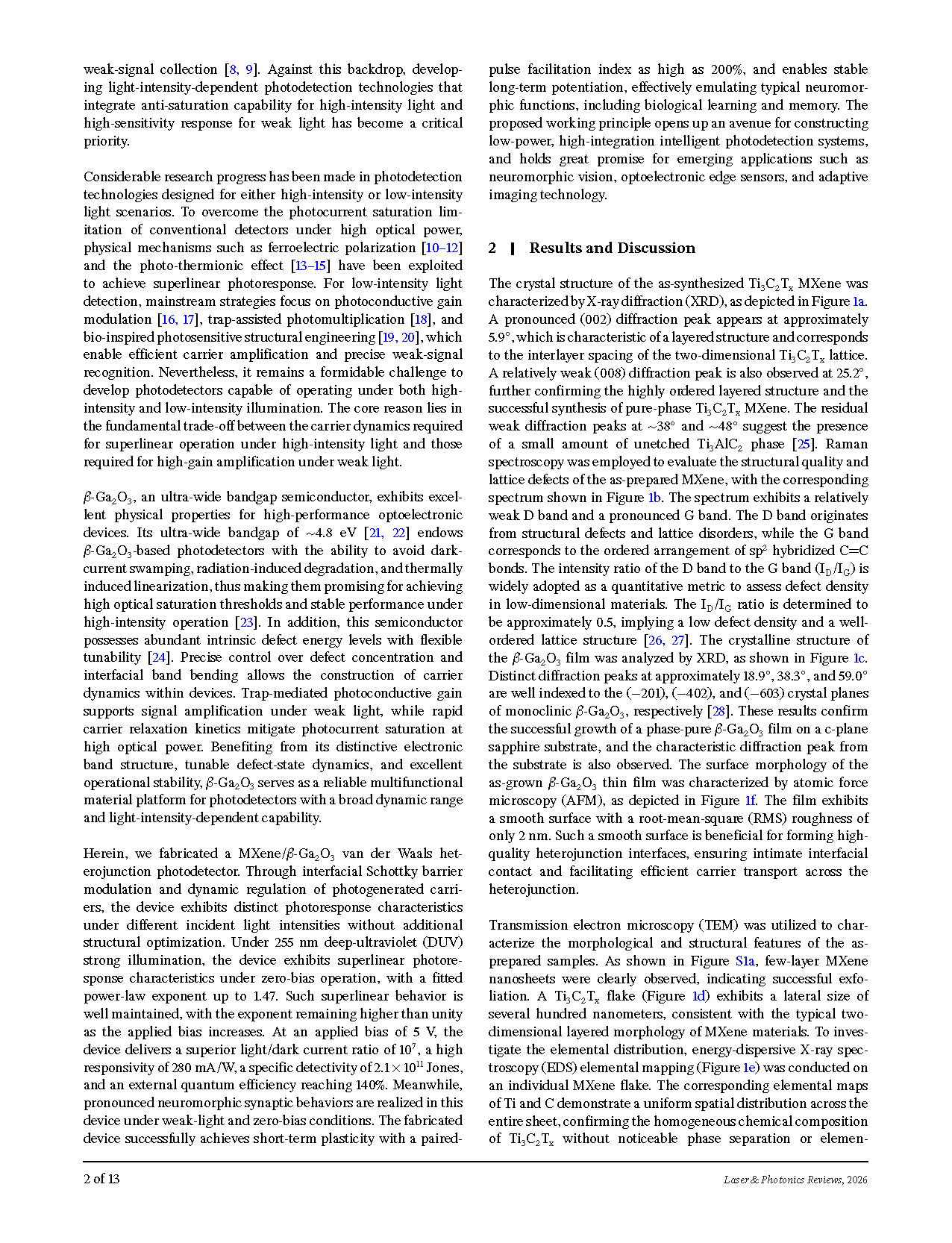
Figure 1. (a) XRD pattern of the Ti₃C₂Tₓ MXene. (b) Raman spectrum of Ti₃C₂Tₓ MXene. (c) XRD pattern of the β‑Ga₂O₃ thin film on c‑plane sapphire. (d) TEM image of Ti₃C₂Tₓ MXene nanosheets. (e) EDS elemental mapping of the Ti₃C₂Tₓ MXene flake. (f) AFM image of the β‑Ga₂O₃ thin film on c‑plane sapphire.
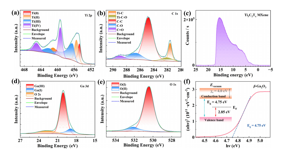
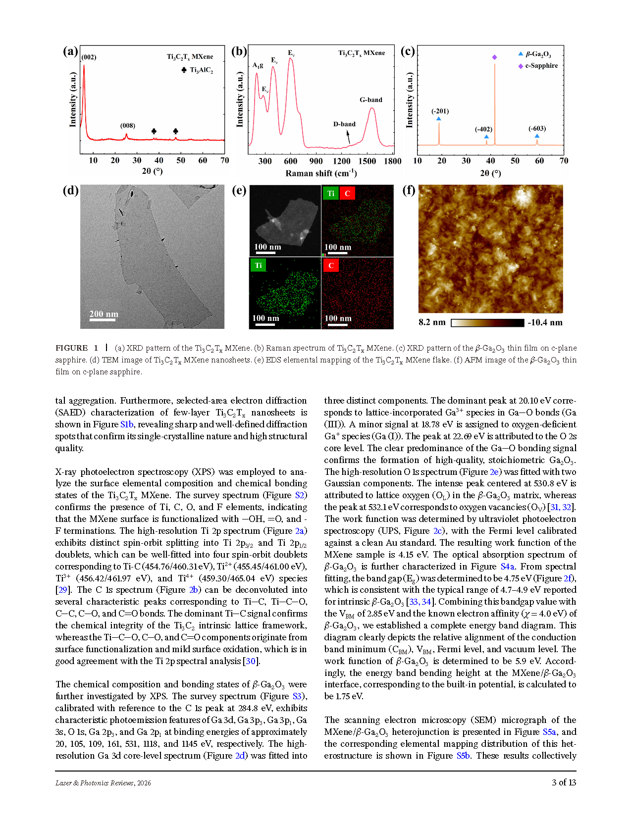
Figure 2. (a) XPS Ti 2p spectrum of the Ti₃C₂Tₓ MXene. (b) XPS C 1s spectrum of the Ti₃C₂Tₓ MXene. (c) UPS spectrum of the Ti₃C₂Tₓ MXene. (d) XPS Ga 3d spectrum of the β‑Ga₂O₃ film. (e) XPS O 1s spectrum of the β‑Ga₂O₃ film. (f) Tauc plot derived from the absorbance data of the β‑Ga₂O₃ sample. The inset shows the corresponding energy band diagram.
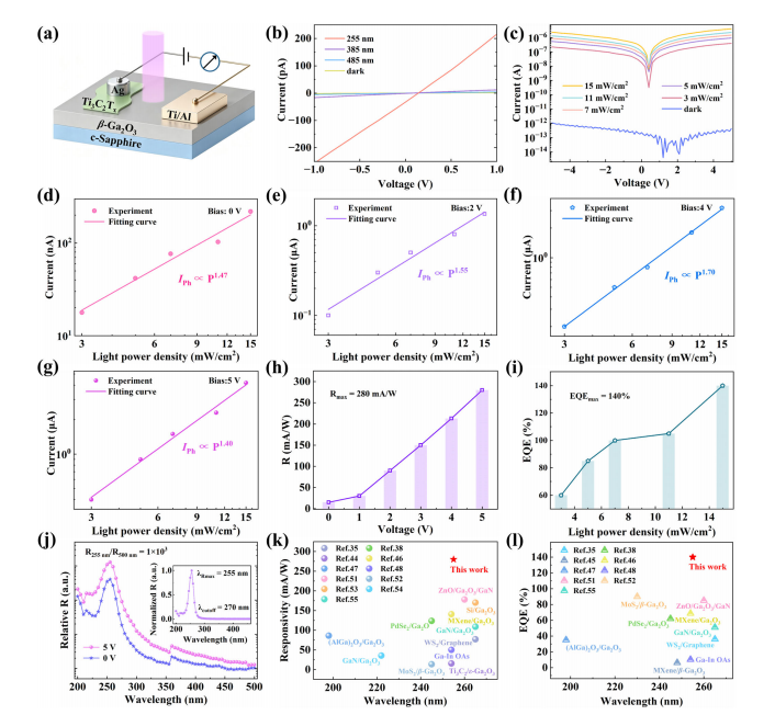
Figure 3. (a) Schematic illustration of the device architecture. (b) I‑V characteristics of the device measured under illumination at 255, 385, and 485 nm, as well as in the dark. (c) I‑V curves under 255 nm illumination at different light power densities, with the dark current shown for comparison. (d) I_ph as a function of incident light power density at zero bias under 255 nm illumination. (e) I_ph versus light power density at bias 2 V. (f) I_ph versus light power density at bias 4 V. (g) I_ph versus light power density at bias 5 V. (h) R as a function of bias voltage under 255 nm illumination. (i) EQE as a function of light power density under 255 nm illumination. (j) Spectral responsivity of the device measured at bias voltages of 0 and 5 V. Inset shows the normalized spectral responsivity. (k) Comparison of R between our device and heterojunction‑based DUV photodetectors in the literature. (l) Comparison of EQE between our device and heterojunction‑based DUV photodetectors in the literature.
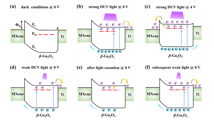
Figure 4. Band diagrams and carrier dynamics of the MXene/β‑Ga₂O₃ heterojunction under (a) dark conditions at zero bias, (b) strong DUV light at zero bias, (c) strong DUV light at a positive bias of 4 V, (d) weak DUV light at zero bias, (e) after light cessation, and (f) subsequent weak light pulse.
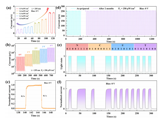
Figure 5. (a) Photocurrent under various light power densities at zero bias. (b) Photocurrent versus bias voltage under fixed light intensity. (c) Temporal response of the device under 1.9 mW/cm² illumination at 0 V bias. (d) Long‑term stability of the photocurrent response over two months. (e) Light pulse sequence for DUV optical communication. (f) Photocurrent response to the binary optical pulse sequence.
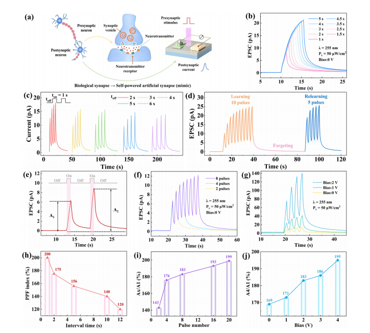
Figure 6. (a) Schematic illustration of a biological synapse and the corresponding self‑powered artificial synapse. (b) EPSC responses under light pulses of varying durations at zero bias. (c) EPSC responses under different inter‑pulse intervals at zero bias. (d) EPSC traces demonstrating the learning‑forgetting‑relearning behavior under successive DUV light pulse stimuli. (e) EPSC responses triggered by two consecutive light pulses at zero bias. (f) EPSC responses versus pulse number at zero bias. (g) EPSC responses versus bias voltages. (h) PPF index (A₂/A₁ ×100 %) as a function of inter‑pulse interval. (i) Normalized EPSC enhancement (Aₓ/A₁ ×100 %) as a function of pulse number. (j) Normalized EPSC ratio (A₄/A₁ ×100 %) as a function of bias voltage.
DOI:
10.1002/lpor.72150

Instruction
Official Account

Cooperation
Top