


Researchers from Cornell University have published a dissertation titled "Observation of quantum oscillations in triethylaluminum-enabled low-temperature MOCVD-grown β-(AlₓGa₁₋ₓ)₂O₃/β-Ga₂O₃ 2DEGs" in Applied Physics Letters.
Background
β-Ga₂O₃ possesses ultra-wide bandgap and exhibits great potential for next-generation radio-frequency power electronic devices. Modulation-doped β-(AlₓGa₁₋ₓ)₂O₃/β-Ga₂O₃ heterostructures can form two-dimensional electron gas, which acts as the core structure for gallium-oxide-based high electron mobility transistors. Although molecular beam epitaxy can realize high-quality fabrication of such heterostructures, its high equipment cost hinders large-scale deployment. Metal-organic chemical vapor deposition (MOCVD) is more suitable for mass production over large areas. When conventional trimethylaluminum is adopted as aluminum precursor, carbon impurities are easily incorporated, which may induce film roughening, cracking and dopant compensation. Reducing growth temperature can be compatible with composite thermal-management substrates for radio-frequency devices, however, fabrication of high-quality β-(AlₓGa₁₋ₓ)₂O₃ epilayers at low temperature via MOCVD still faces obstacles. Meanwhile, for MOCVD-grown 2DEG in this material system, experimental evidence for Shubnikov-de Haas quantum oscillations — the signature of high-quality transport — as well as low-temperature transport limits and dominant scattering mechanisms remain insufficient, which restricts further development of MOCVD processes for Ga₂O₃ radio-frequency devices.
Abstract
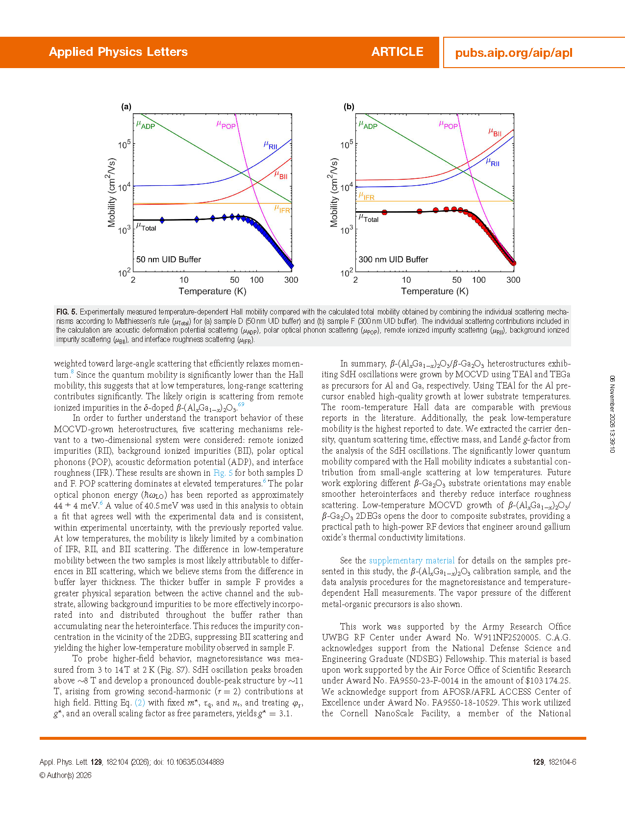
We report the observation of Shubnikov–de Haas (SdH) oscillations in metal-organic chemical vapor deposition (MOCVD)-grown (010)-oriented β-(AlₓGa₁₋ₓ)₂O₃/β-Ga₂O₃ modulation δ-doped heterostructures. Triethylgallium (TEGa) and triethylaluminum (TEAl) were used as precursors, which enabled the growth to occur at a relatively low substrate temperature of 650 °C. The as-grown films exhibit sub-nanometer roughness and show distinct Laue oscillations, confirming a high-quality, sharp heterointerface. Additionally, we report the highest β-(AlₓGa₁₋ₓ)₂O₃/β-Ga₂O₃ two-dimensional electron gas (2DEG) low-temperature mobility to date of 2914 cm²/Vs at 45 K. From the SdH oscillations below 10 K, we extract a 2DEG density of 1.7 × 10¹² cm⁻², a cyclotron effective mass of 0.305 ± 0.007 mₑ, a quantum scattering time of 178 ± 11 fs, and an estimated effective g-factor of 3.1. The effective mass is in reasonable agreement with the calculated conduction band nonparabolicity in β-Ga₂O₃ given the estimated position of the Fermi level above the conduction band minimum. Temperature-dependent transport is further analyzed to determine that background and remote ionized impurity scattering are the likely dominant scattering mechanisms at low temperatures. This work affirms the viability of MOCVD using TEAl and TEGa for growing high-quality gallium-oxide-based heterostructures.
Highlights
Realize low-temperature (650 °C) MOCVD growth of δ-doped β-(AlₓGa₁₋ₓ)₂O₃/β-Ga₂O₃heterostructures adopting TEAl and TEGa precursors, achieving sharp heterointerface with sub-nm roughness.
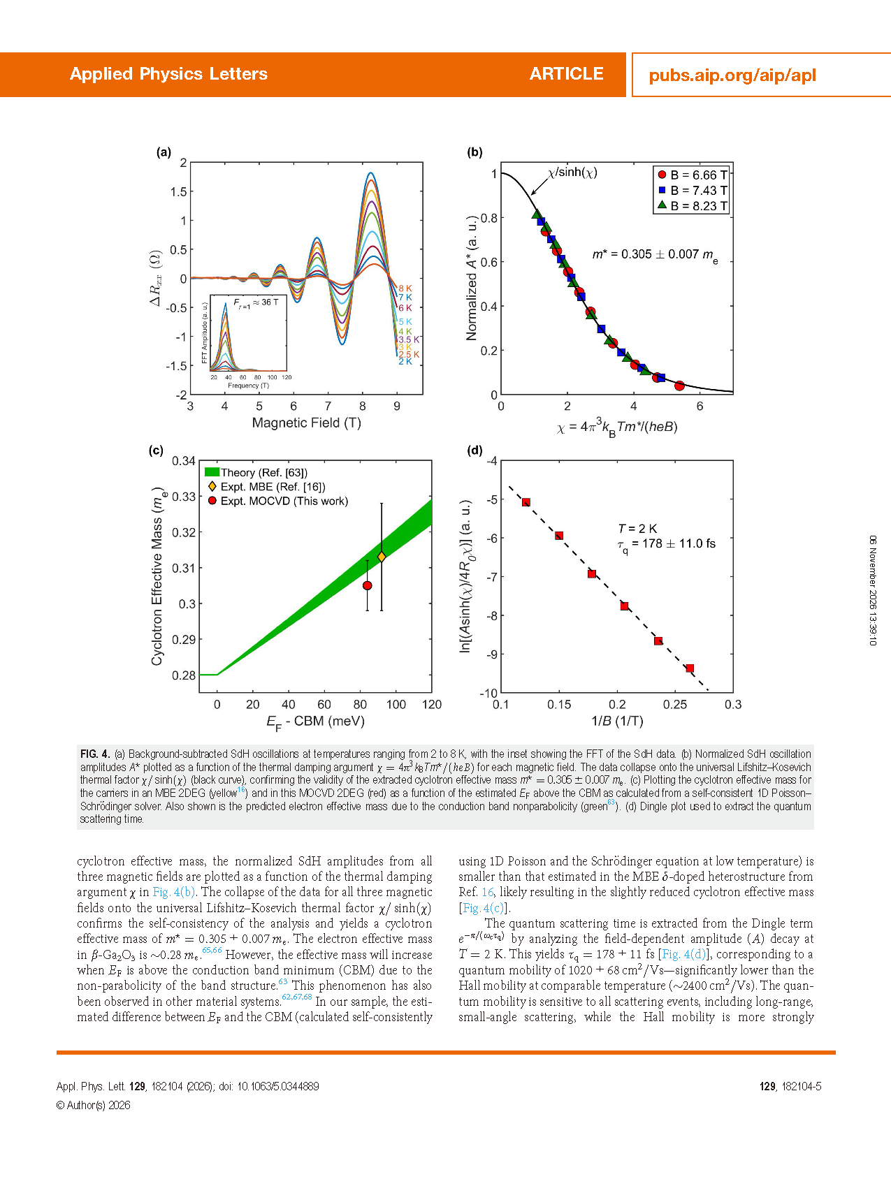
Observe Shubnikov-de Haas quantum oscillations in MOCVD-grown β-Ga₂O₃-based 2DEG, extract 2DEG density, cyclotron effective mass, quantum scattering time and effective g-factor.
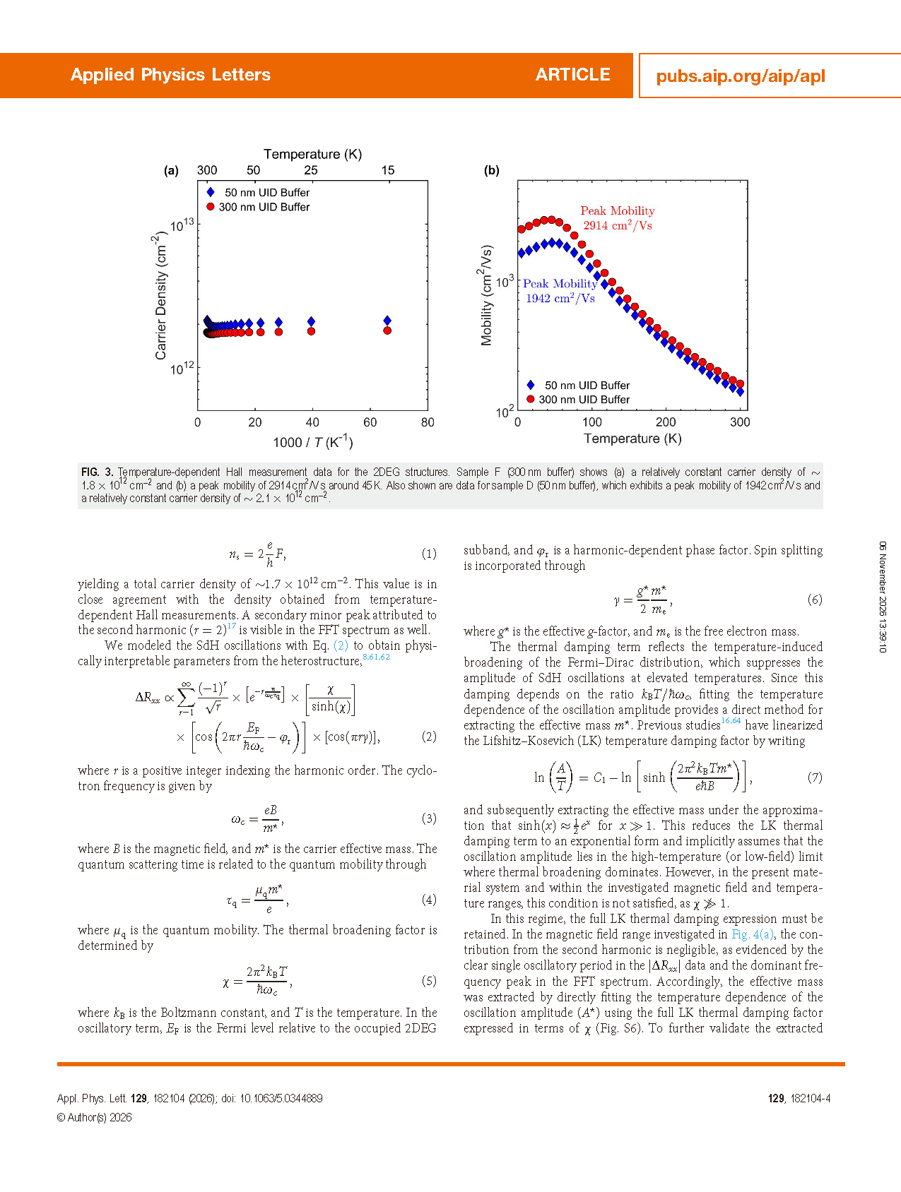
Obtain record-high low-temperature mobility of 2914 cm²/Vs at 45 K for MOCVD-grown β-(AlₓGa₁₋ₓ)₂O₃/β-Ga₂O₃2DEG.
Clarify that background and remote ionized impurity scattering dominate the low-temperature transport properties of the 2DEG.
Conclusion
In summary, β-(AlₓGa₁₋ₓ)₂O₃/β-Ga₂O₃ heterostructures exhibiting SdH oscillations were grown by MOCVD using TEAl and TEGa as precursors for Al and Ga, respectively. Using TEAl for the Al precursor enabled high-quality growth at lower substrate temperatures. The room-temperature Hall data are comparable with previous reports in the literature. Additionally, the peak low-temperature mobility is the highest reported to date. We extracted the carrier density, quantum scattering time, effective mass, and Lande g-factor from the analysis of the SdH oscillations. The significantly lower quantum mobility compared with the Hall mobility indicates a substantial contribution from small-angle scattering at low temperatures. Future work exploring different β-Ga₂O₃ substrate orientations may enable smoother heterointerfaces and thereby reduce interface roughness scattering. Low-temperature MOCVD growth of β-(AlₓGa₁₋ₓ)₂O₃/β-Ga₂O₃ 2DEGs opens the door to composite substrates, providing a practical path to high-power RF devices that engineer around gallium oxide’s thermal conductivity limitations.
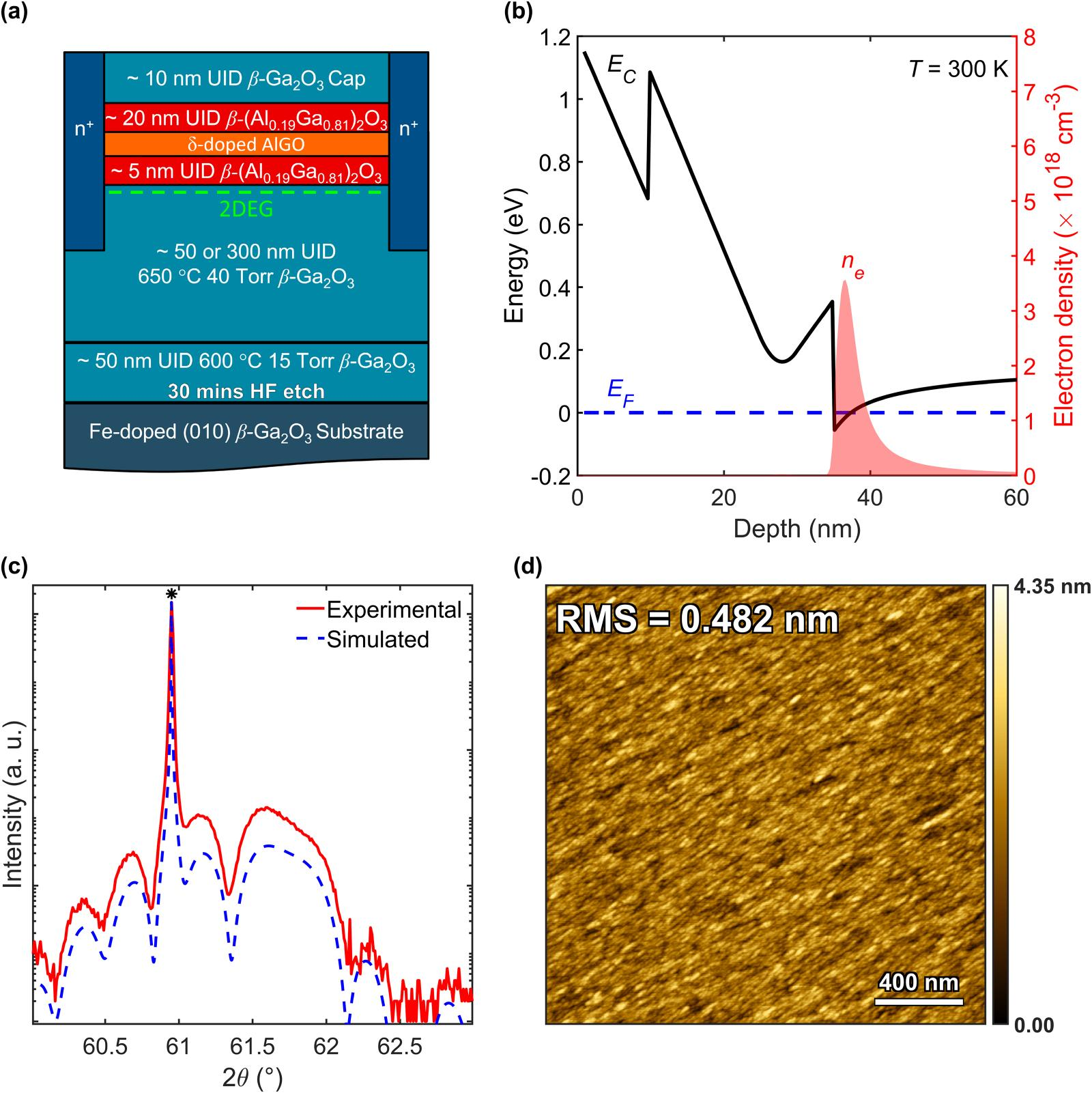
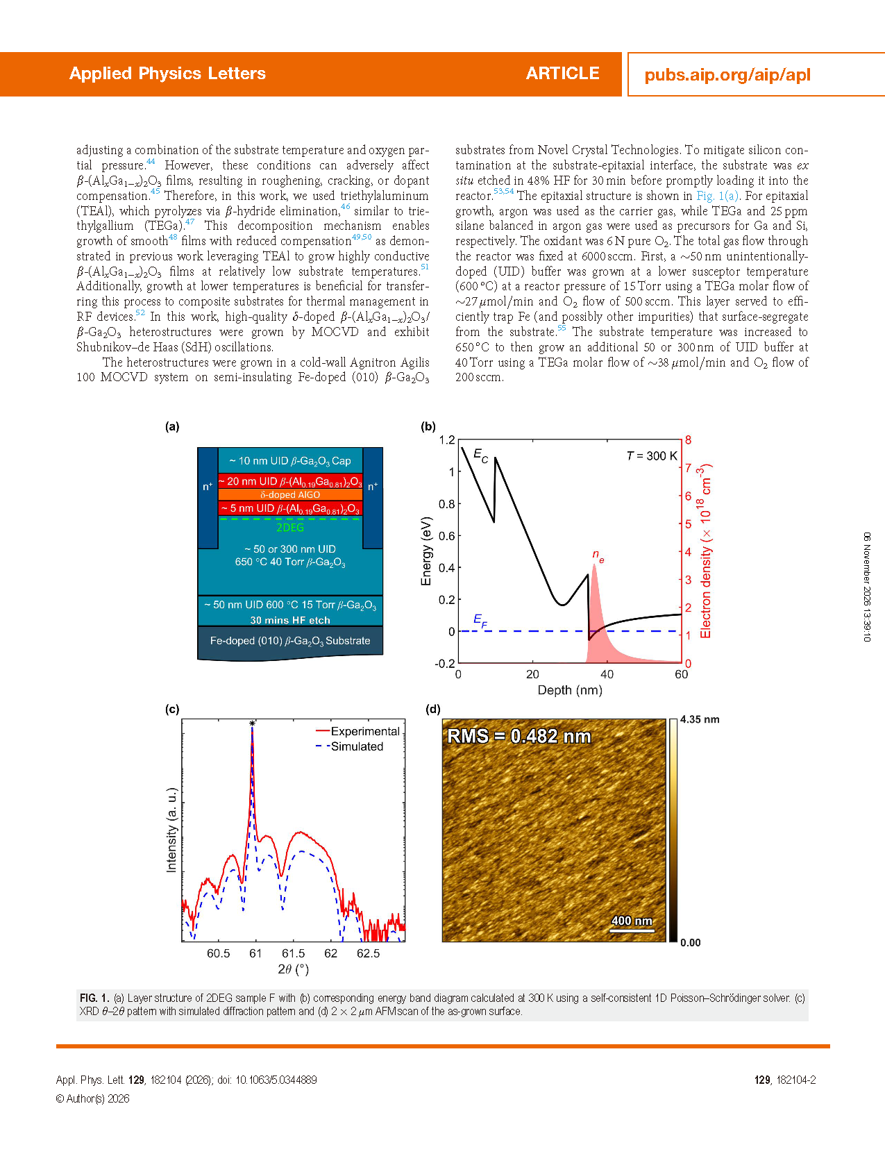
FIG. 1. (a) Layer structure of 2DEG sample F with (b) corresponding energy band diagram calculated at 300 K using a self-consistent 1D Poisson–Schrödinger solver. (c) XRD θ–2θ pattern with simulated diffraction pattern and (d) 2 × 2 μm AFM scan of the as-grown surface.
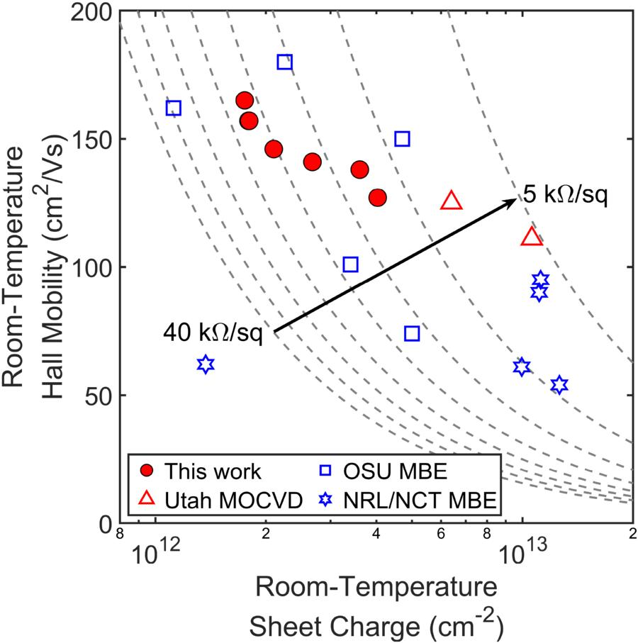
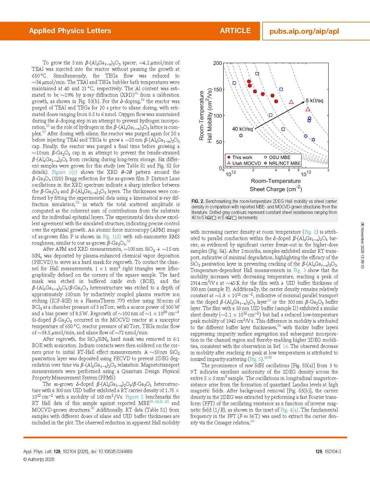
FIG. 2. Benchmarking the room-temperature 2DEG Hall mobility vs sheet carrier density in comparison with reported MBE- and MOCVD-grown structures from the literature. Dotted gray contours represent constant sheet resistances ranging from 40 to 5 kΩ/□ in 5 kΩ/□ increments.
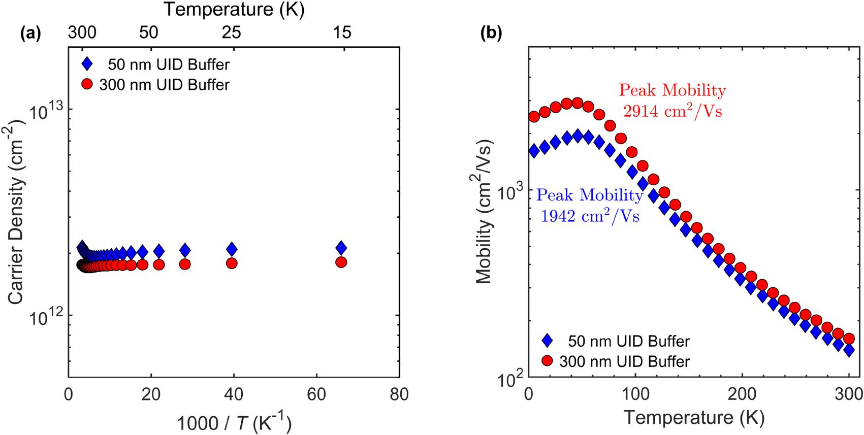
FIG. 3. Temperature-dependent Hall measurement data for the 2DEG structures. Sample F (300 nm buffer) shows (a) a relatively constant carrier density of 1.8 × 10¹² cm⁻² and (b) a peak mobility of 2914 cm²/Vs around 45 K. Also shown are data for sample D (50 nm buffer), which exhibits a peak mobility of 1942 cm²/Vs and a relatively constant carrier density of ~ 2.1 × 10¹² cm⁻².
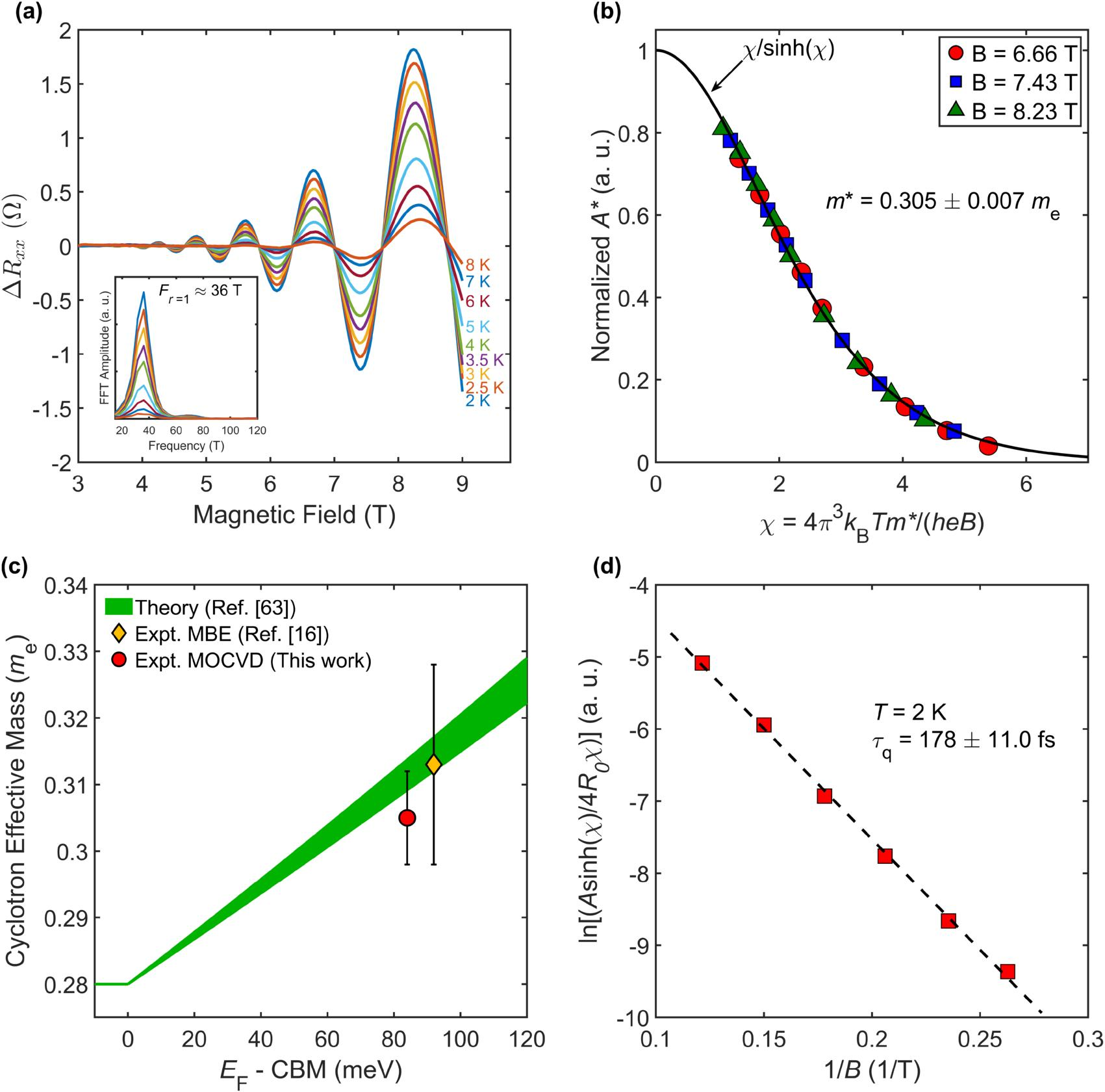
FIG. 4. (a) Background-subtracted SdH oscillations at temperatures ranging from 2 to 8 K, with the inset showing the FFT of the SdH data. (b) Normalized SdH oscillation amplitudes A* plotted as a function of the thermal damping argument χ = 4π³kBTm*/(heB) for each magnetic field. The data collapse onto the universal Lifshitz–Kosevich thermal factor χ/sinh (χ) (black curve), confirming the validity of the extracted cyclotron effective mass m* = 0.305 ± 0.007 me. (c) Plotting the cyclotron effective mass for the carriers in an MBE 2DEG (yellow) and in this MOCVD 2DEG (red) as a function of the estimated EF above the CBM as calculated from a self-consistent 1D Poisson–Schrödinger solver. Also shown is the predicted electron effective mass due to the conduction band nonparabolicity (green). (d) Dingle plot used to extract the quantum scattering time.
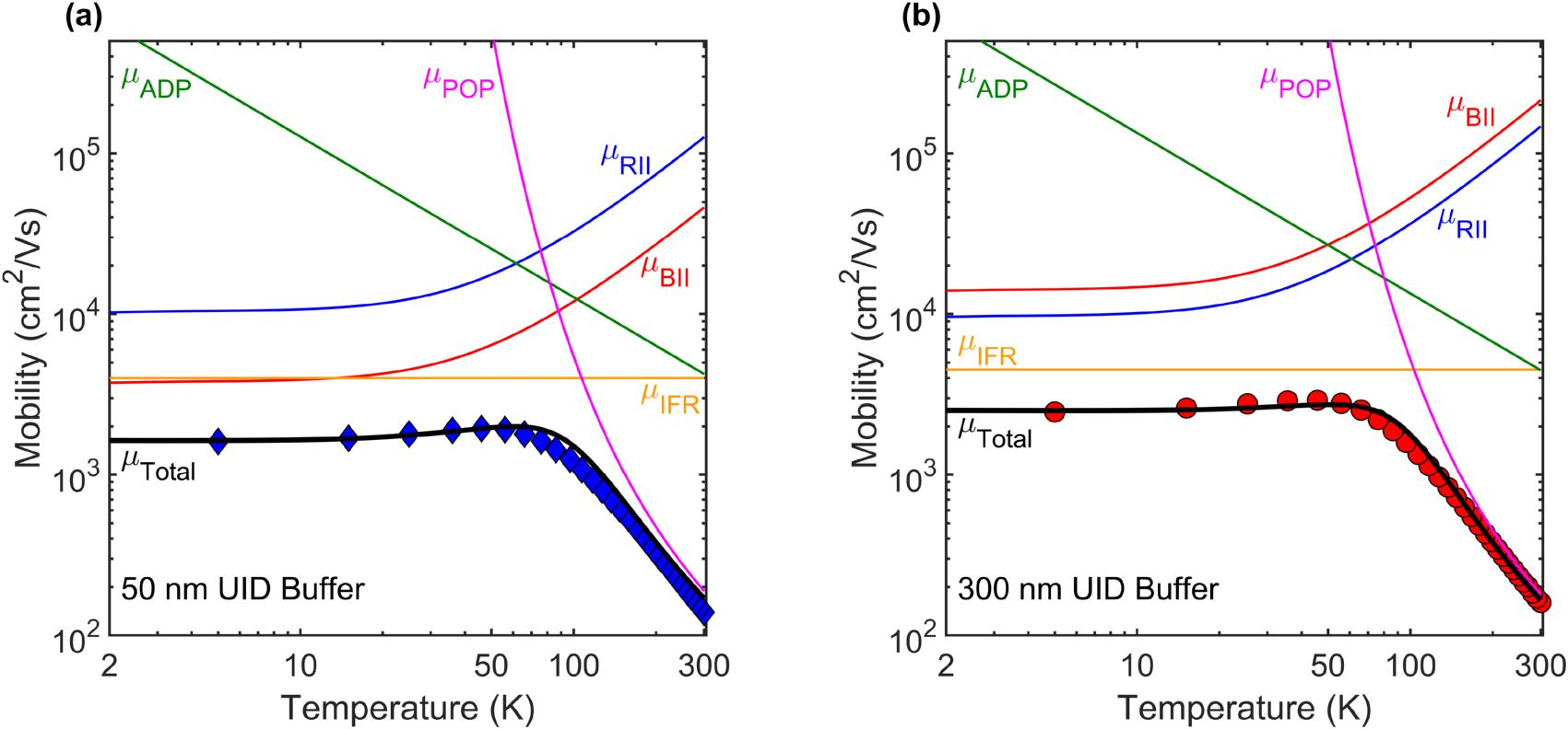
FIG. 5. Experimentally measured temperature-dependent Hall mobility compared with the calculated total mobility obtained by combining the individual scattering mechanisms according to Matthiessen’s rule (μTotal) for (a) sample D (50 nm UID buffer) and (b) sample F (300 nm UID buffer). The individual scattering contributions included in the calculation are acoustic deformation potential scattering (μADP), polar optical phonon scattering (μPOP), remote ionized impurity scattering (μRII), background ionized impurity scattering (μBII), and interface roughness scattering (μIFR).
DOI:
doi.org/10.1063/5.0344889
Instruction
Official Account

Cooperation
Top