


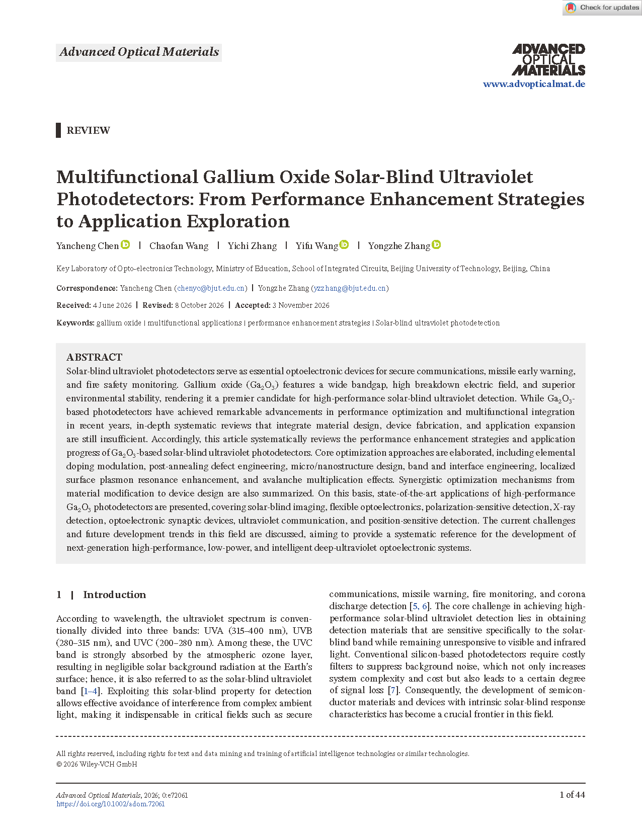
Recently, the team led by Yancheng Chen and Yongzhe Zhangat the School of Integrated Circuits, Beijing University of Technology, published a review article in Advanced Optical Materials, systematically reviewing the performance-enhancement strategies and application advances of Ga2O3-based solar-blind ultraviolet photodetectors. Following the main thread of “material design-device fabrication-application expansion,” the article summarizes multiple optimization pathways, ranging from elemental doping, defect engineering, micro/nanostructures, and band and interface engineering to localized surface plasmon resonance (LSPR) and avalanche multiplication. It also outlines prospects for frontier applications such as solar-blind imaging, flexible optoelectronics, polarization detection, X-ray detection, optoelectronic synapses, ultraviolet communication, and position-sensitive detection.
Paper Information: Yancheng Chen, Chaofan Wang, Yichi Zhang, Yifu Wang, Yongzhe Zhang, Multifunctional Gallium Oxide Solar-Blind Ultraviolet Photodetectors: From Performance Enhancement Strategies to Application Exploration, Advanced Optical Materials, 2026, e72061. DOI: 10.1002/adom.72061.
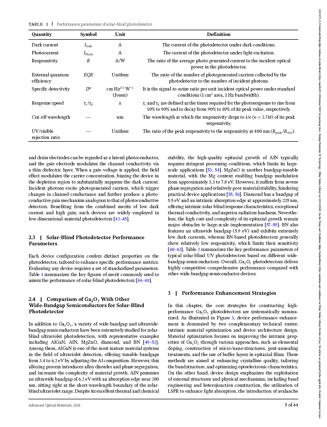
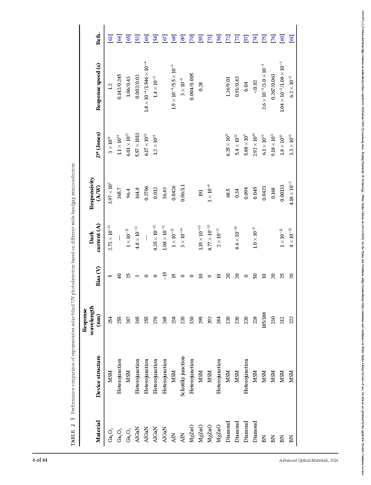
Solar-blind ultraviolet detection has irreplaceable value in scenarios such as secure communication, missile warning, fire monitoring, and corona discharge detection. Ga2O3 has an ultra-wide bandgap of approximately 4.4–5.3 eV, and its intrinsic absorption edge falls exactly within the 200–280 nm solar-blind band. It also possesses a high breakdown electric field, excellent chemical and thermal stability, and relatively low manufacturing cost, and is therefore regarded as a “star material” for high-performance solar-blind ultraviolet detection. However, how to move from single-performance optimization toward multifunctional system integration remains a core issue facing the field.
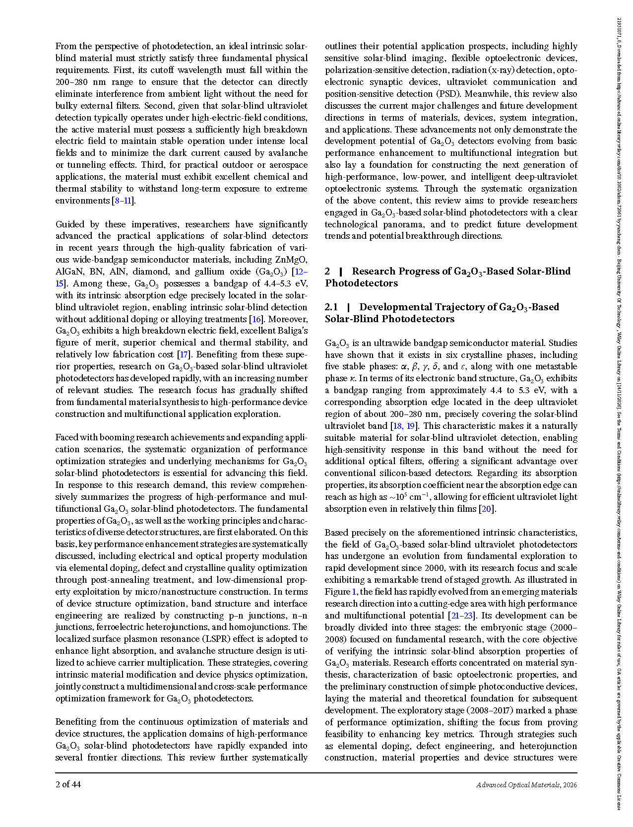
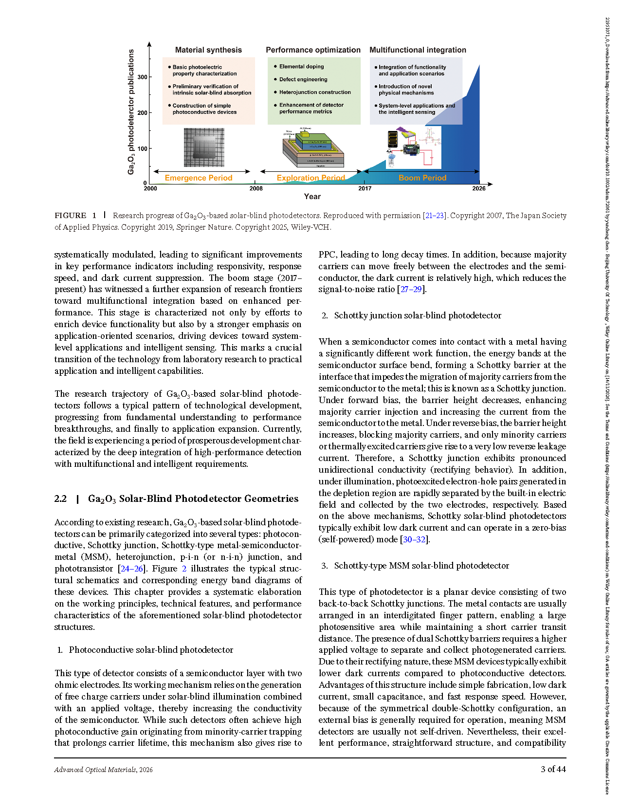
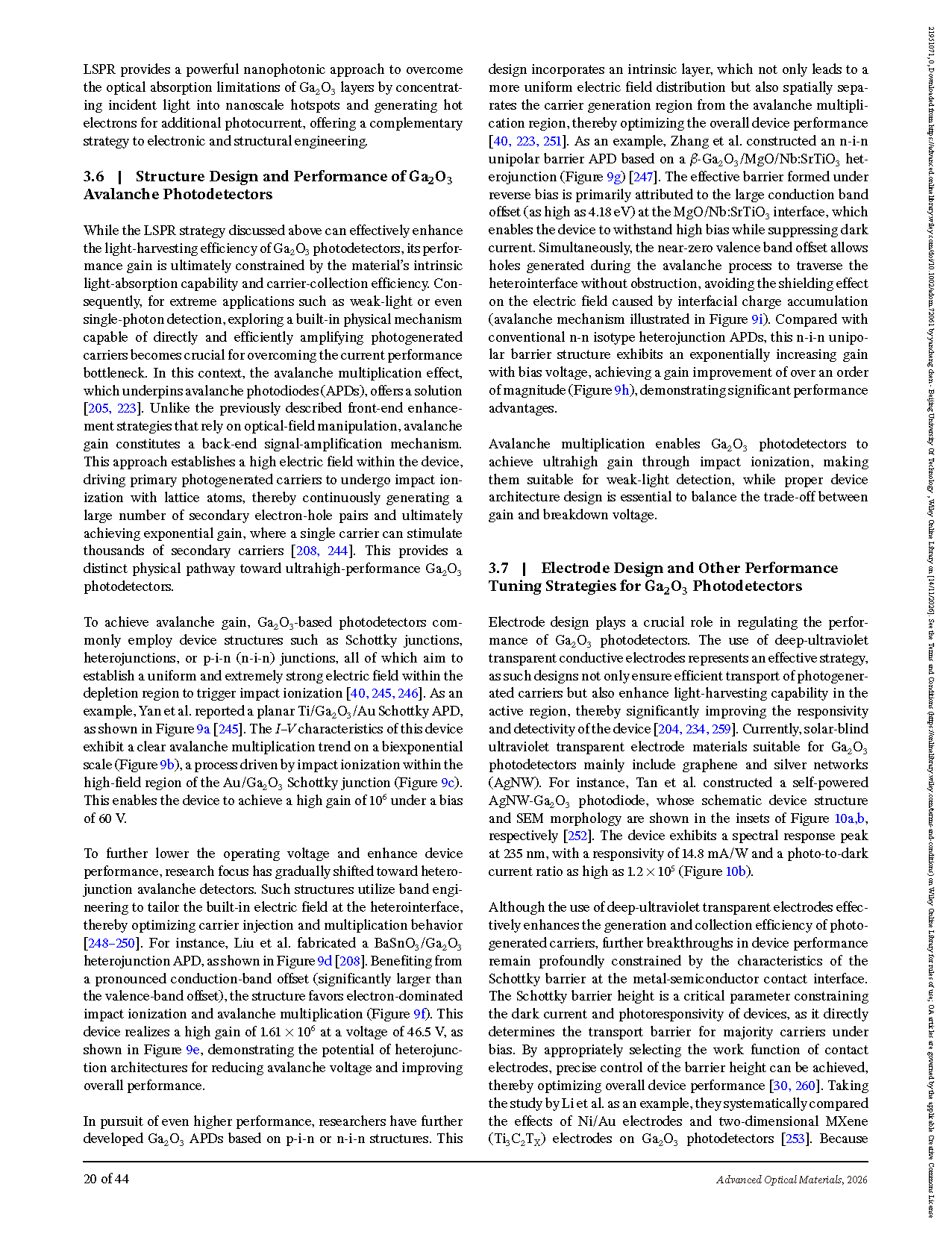
The article first divides the development of Ga2O3 solar-blind photodetectors into three stages: the embryonic period (2000–2008), which focused on material synthesis and verification of intrinsic solar-blind absorption; the exploratory period (2008–2017), in which doping, defect engineering, and heterostructure construction were used to improve responsivity and response speed and to suppress dark current; and the prosperity period (2017–present), which has shifted toward multifunctional integration and system-level applications, driving devices from the laboratory toward intelligent sensing.
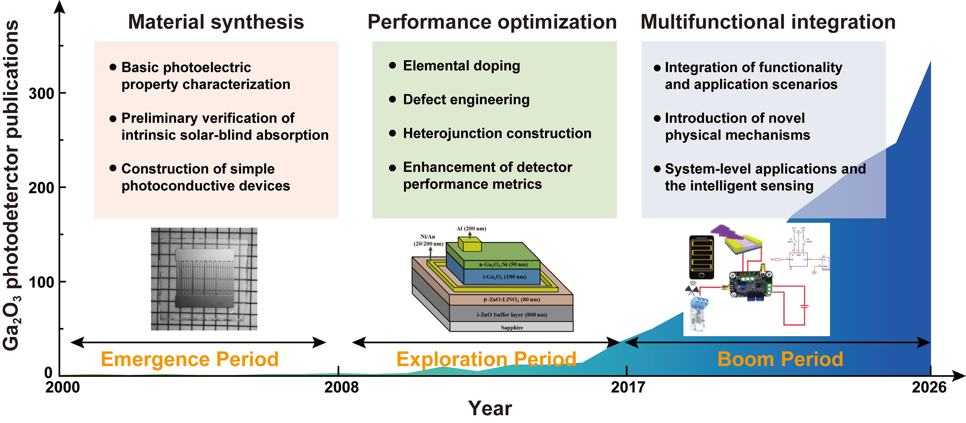
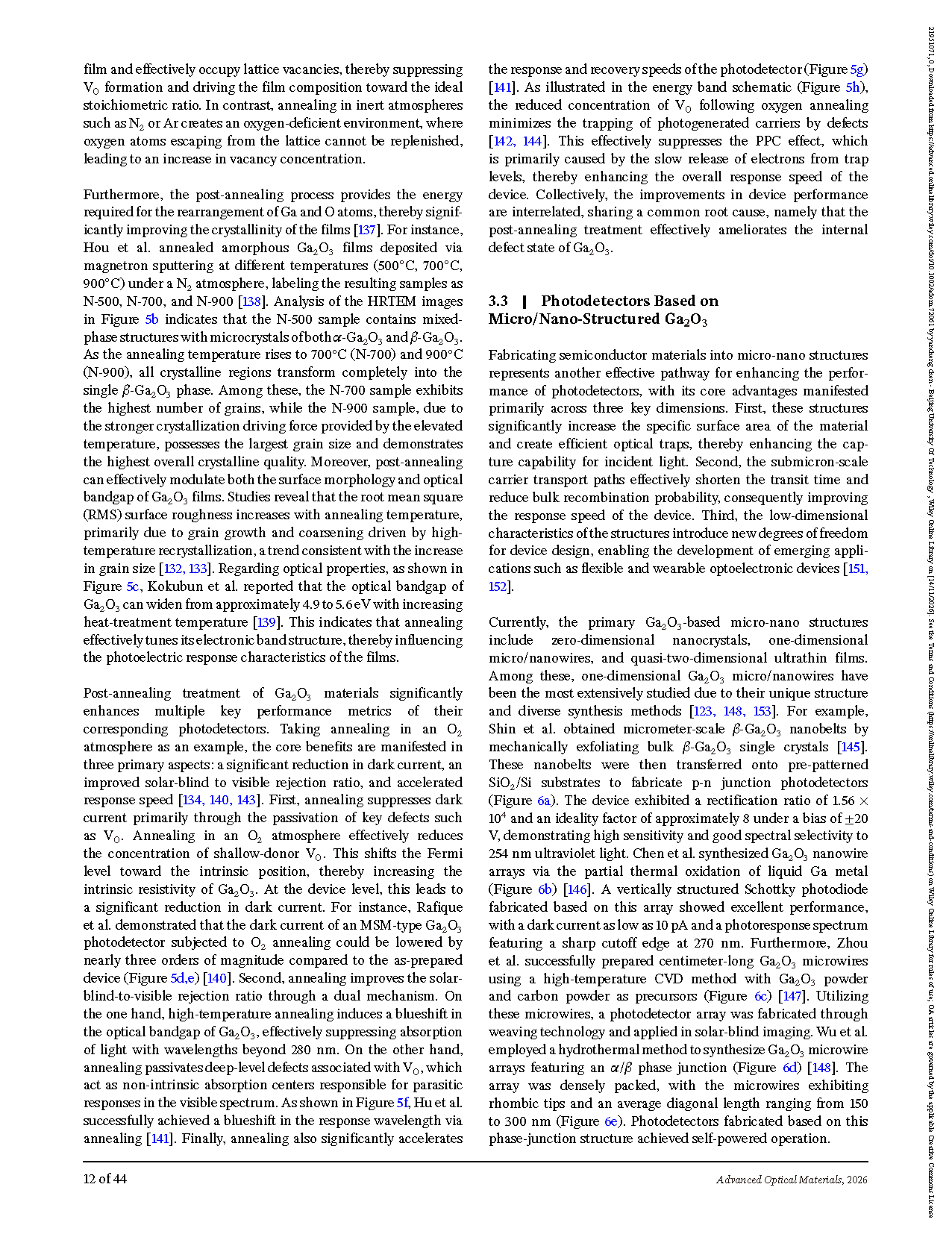
Fig. 1 Research progress of Ga2O3 solar-blind photodetectors
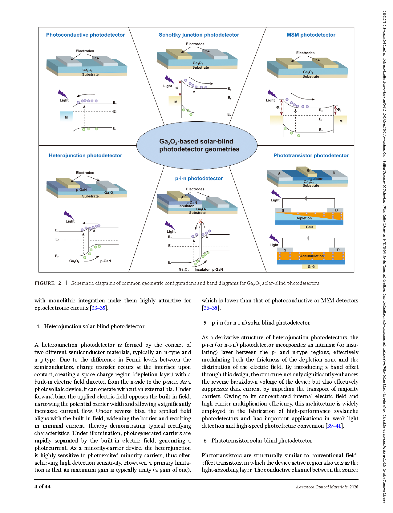
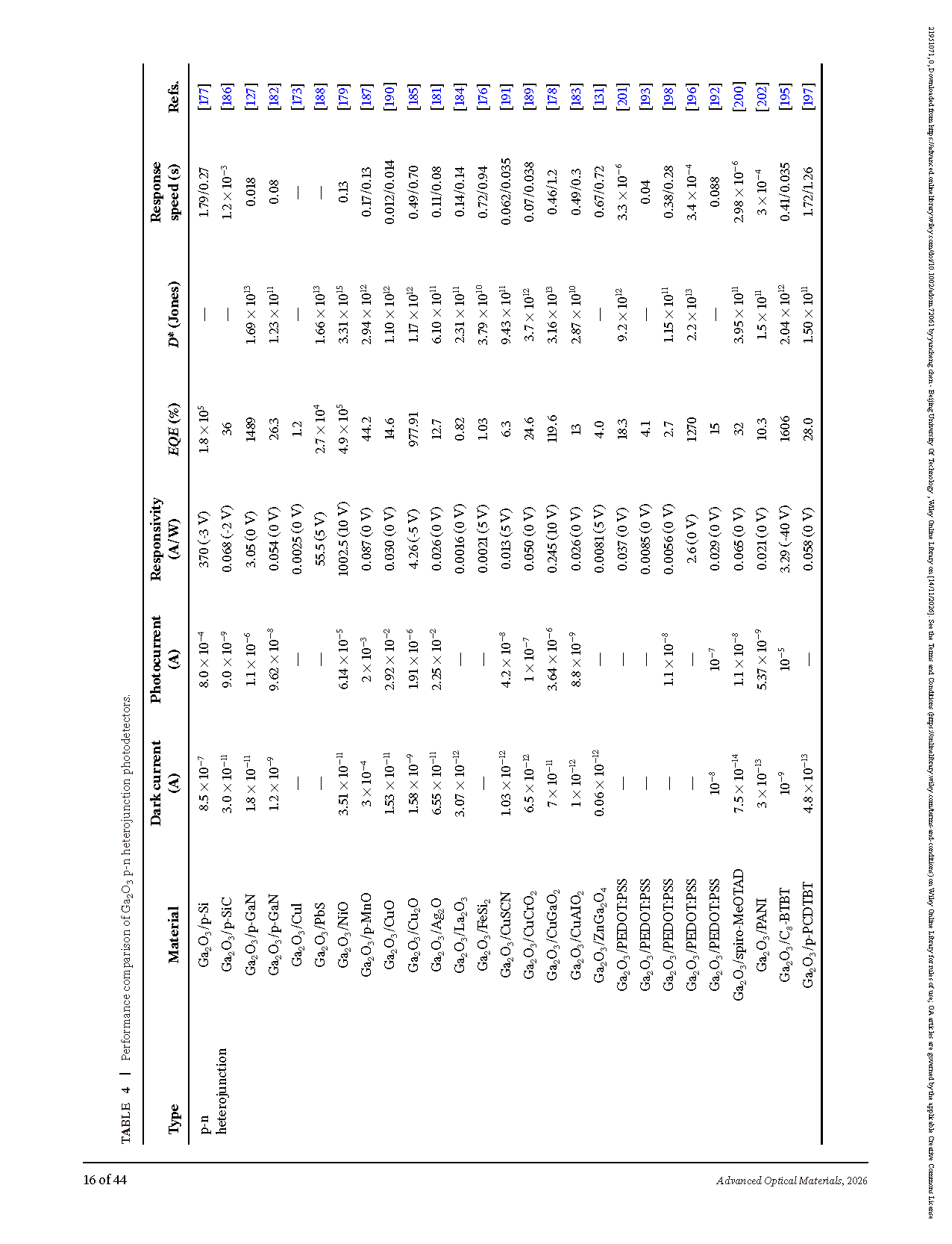
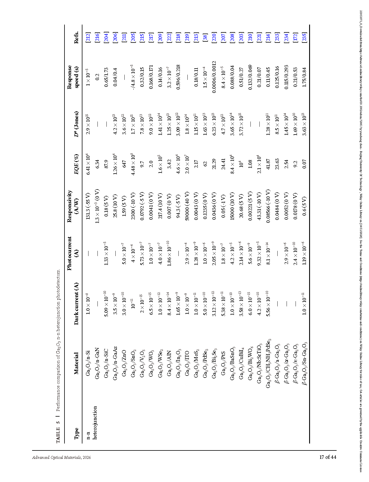
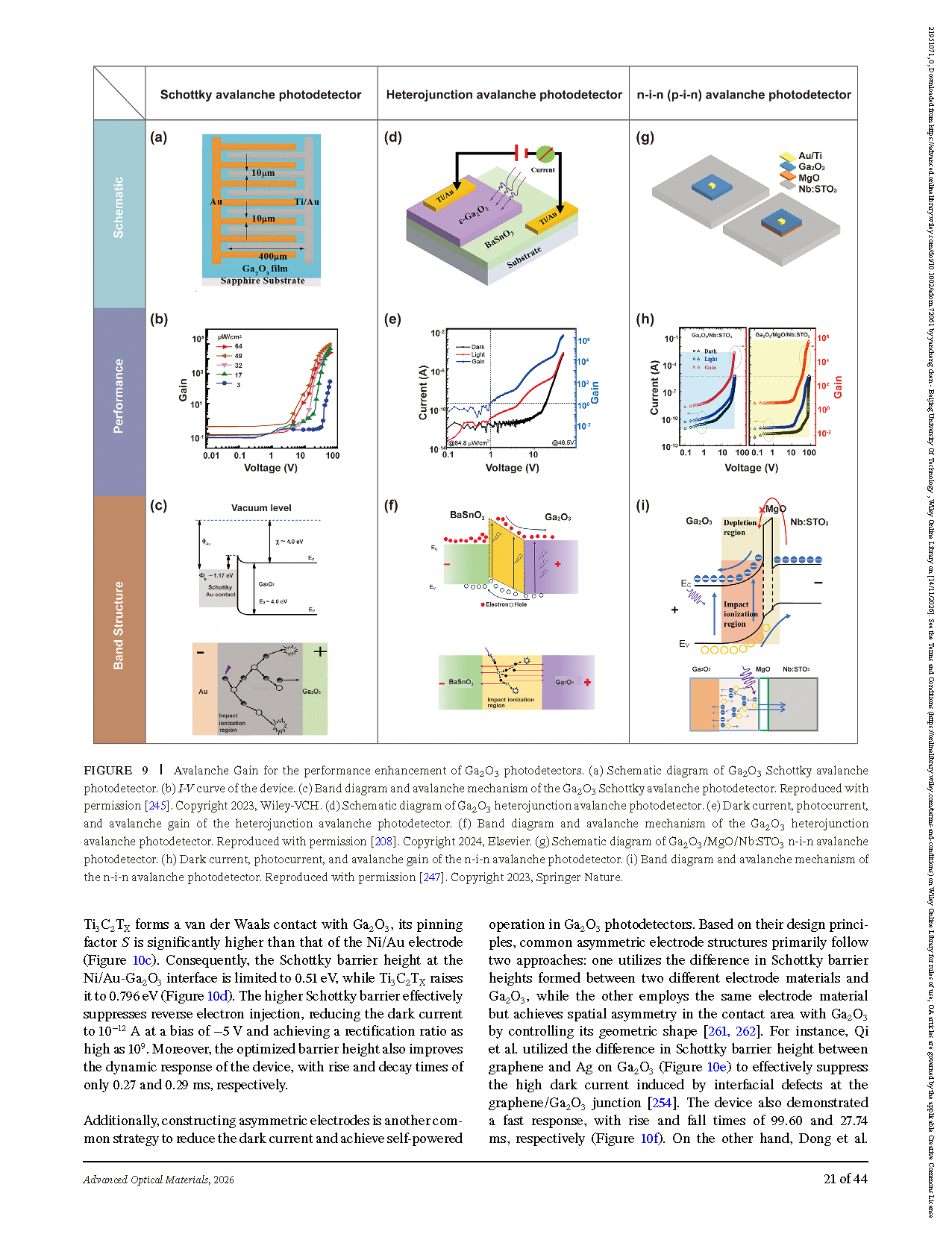
In terms of device structures, the review systematically compares the principles, advantages, and limitations of configurations such as photoconductive devices, Schottky junctions, MSM, heterojunctions, p-i-n (n-i-n) structures, and phototransistors. For example, the photoconductive type offers high gain but suffers from large dark current and slow response; Schottky junctions and MSM devices exhibit low dark current and fast response but usually require an applied bias; heterojunctions and p-i-n structures, by contrast, achieve self-powered operation and efficient carrier separation through built-in electric fields.
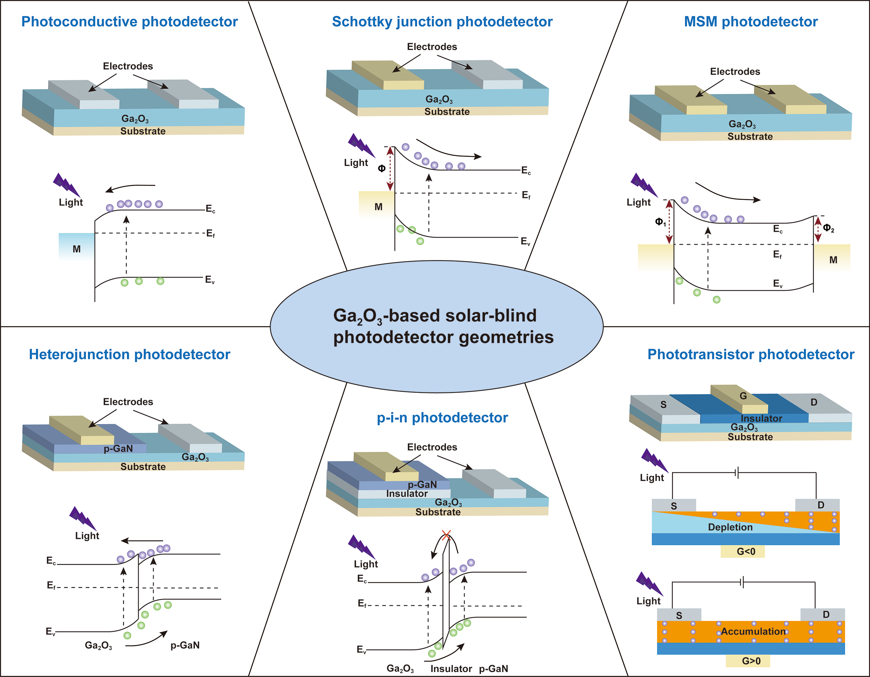
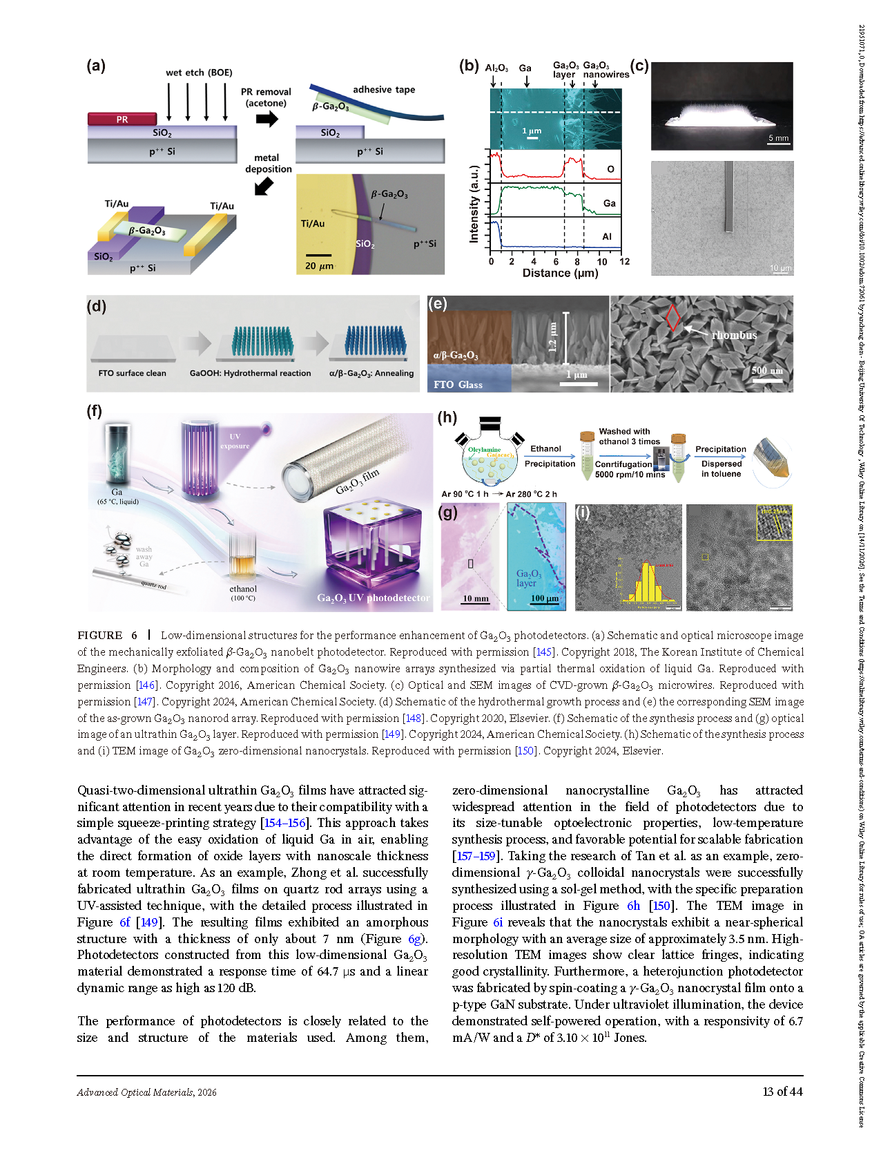
Fig. 2 Common device architectures of Ga2O3 photodetectors.
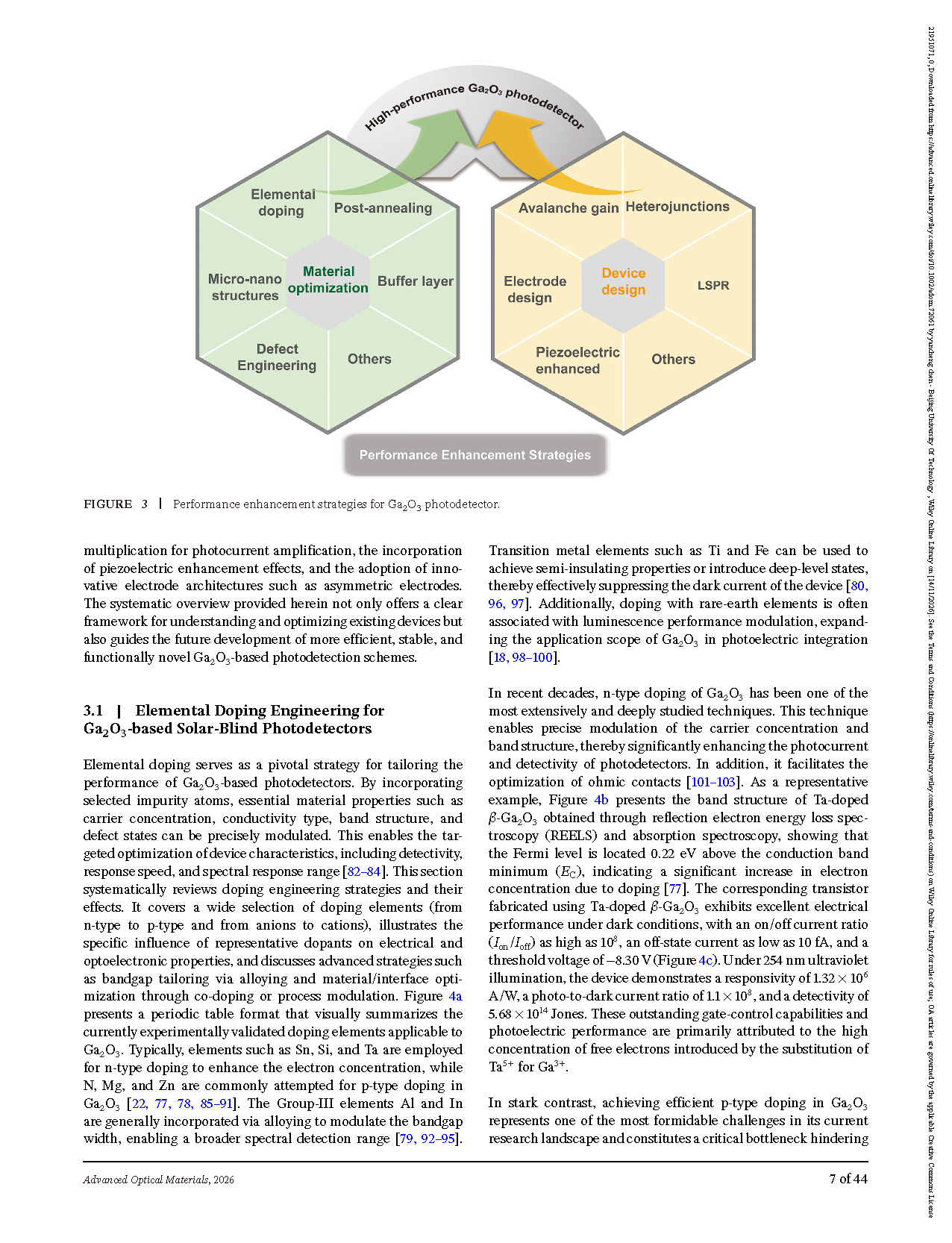
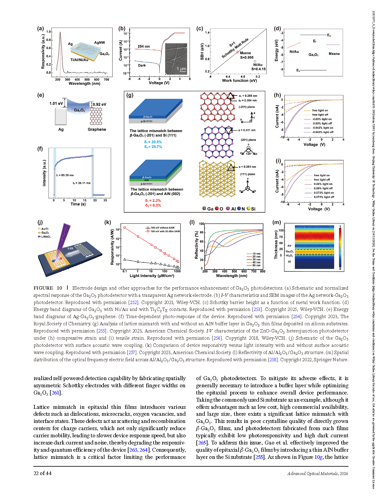
Performance enhancement strategies are the central focus of the review. The article summarizes six core pathways:
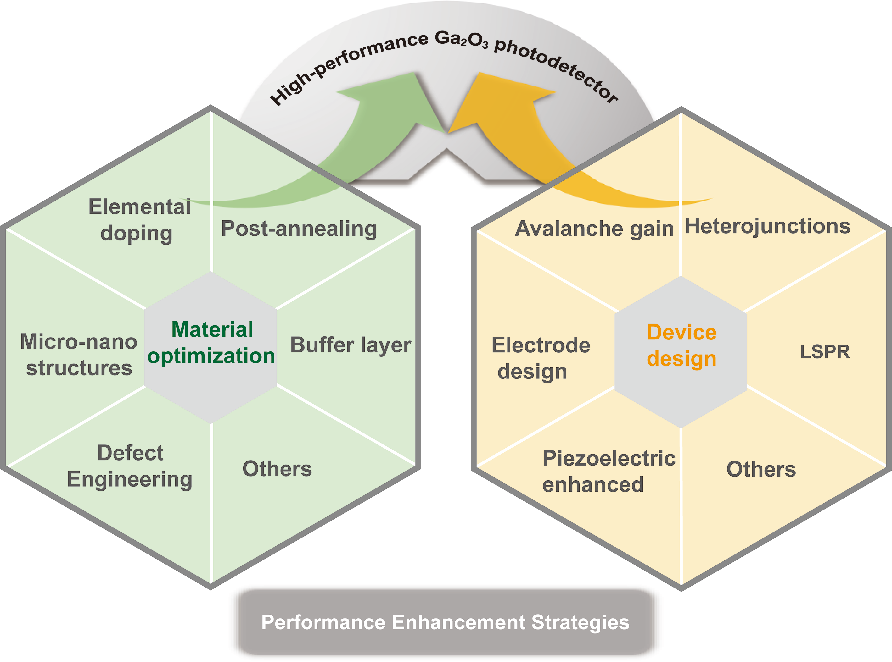
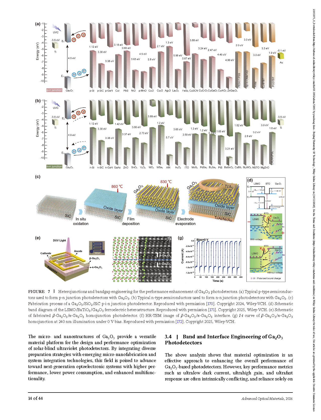
Fig. 3 Performance enhancement strategies for Ga2O3 photodetectors.
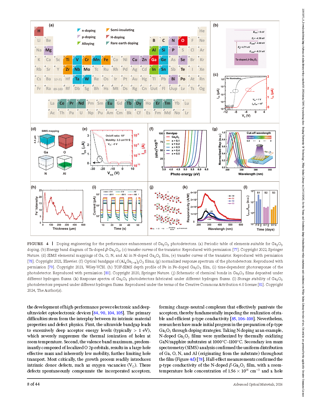
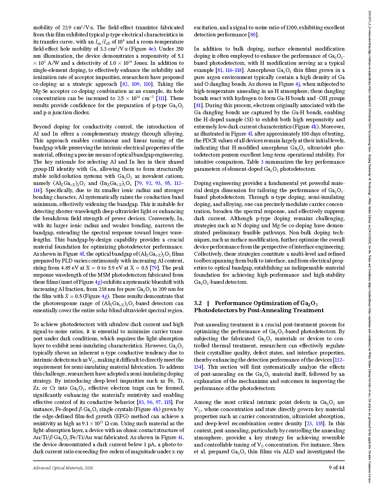
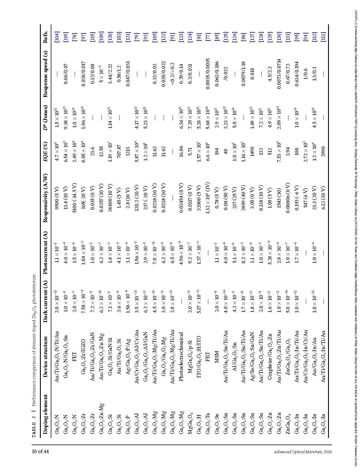
Elemental doping engineering: n-type doping with Sn, Si, Ta, etc. increases electron concentration; p-type doping with N, Mg, Zn, etc. remains challenging but has shown preliminary progress; Al/In alloying enables continuous bandgap tuning; semi-insulating doping with Fe, Ti, Zr, Cr, etc. suppresses dark current; and H surface modification improves the response and stability of amorphous Ga2O3.
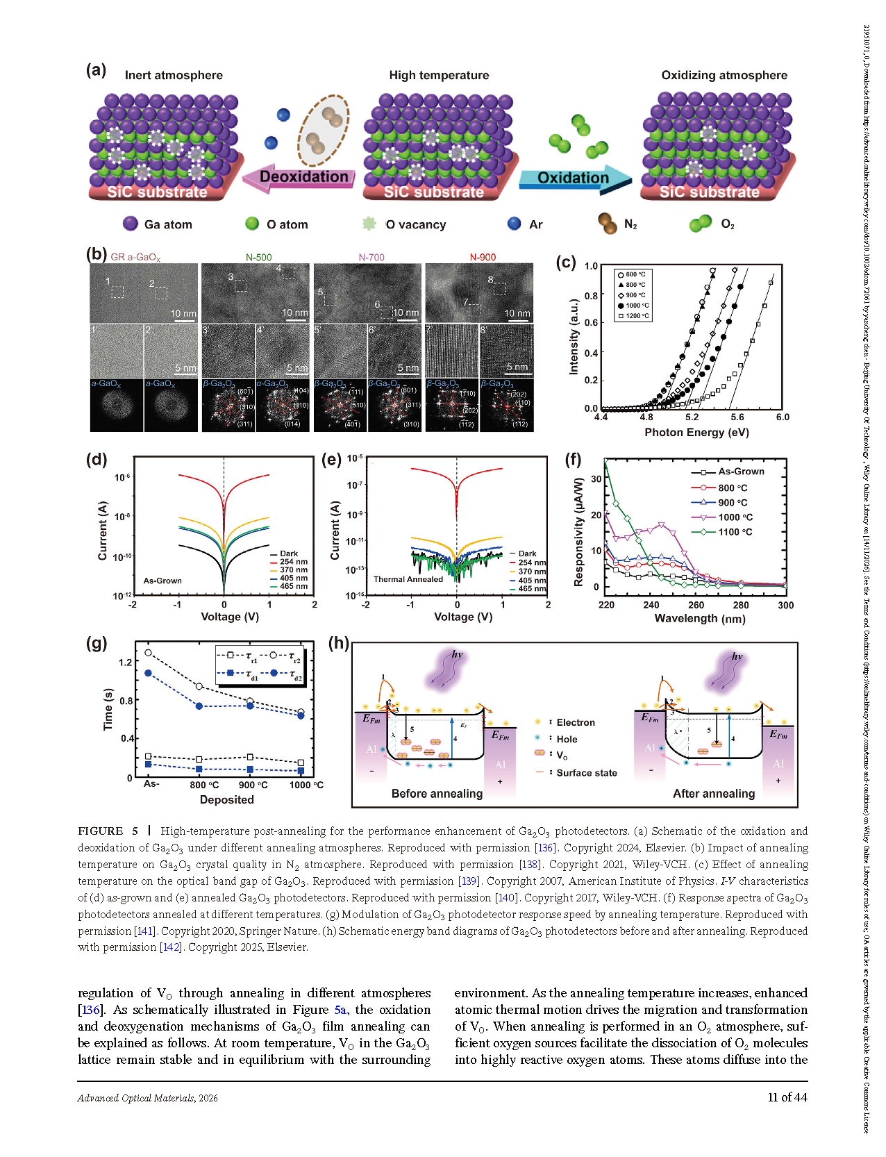
Post-annealing defect engineering: the oxygen vacancy concentration is modulated through atmospheres such as O2, N2, and Ar, thereby improving crystalline quality, reducing dark current, enhancing the solar-blind/visible rejection ratio, and accelerating the response speed.
Micro/nanostructure design: structures such as nanobelts, nanowire arrays, microwires, ultrathin Ga2O3films, and zero-dimensional quantum dots improve performance by increasing the specific surface area, shortening carrier transport paths, and enhancing light trapping.
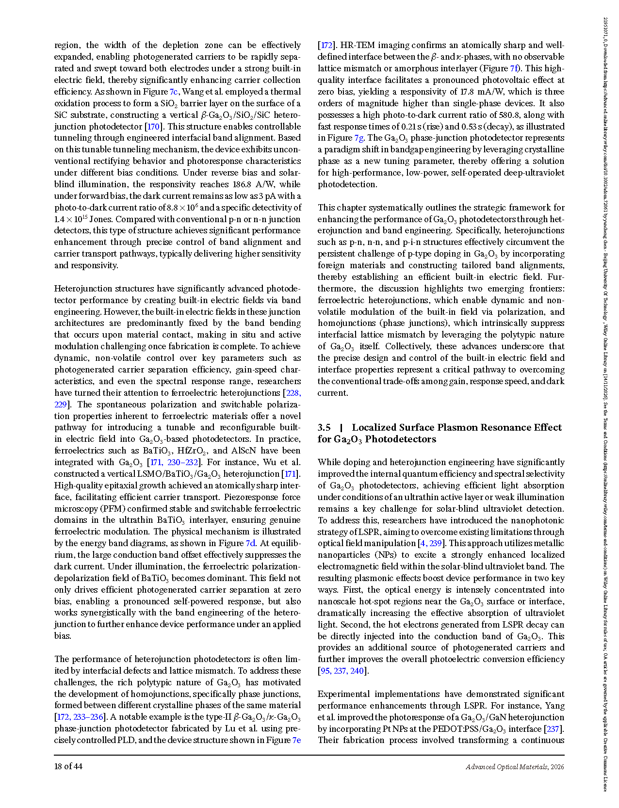
Band and interface engineering: p-n, n-n, and p-i-n heterojunctions, ferroelectric heterojunctions, and β/κ-Ga2O3homophase junctions are constructed, and built-in electric fields and band alignment are utilized to achieve efficient carrier separation and dark current suppression.
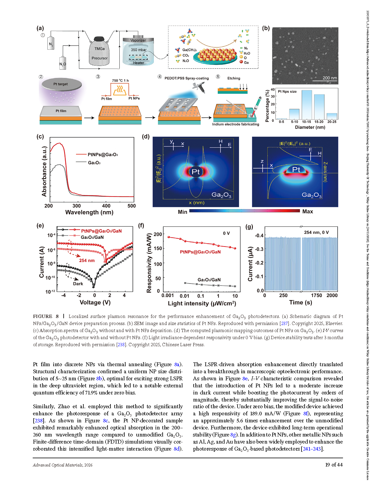
LSPR enhancement: localized surface plasmon resonance of metal nanoparticles such as Pt, Al, Ag, and Au in the deep-ultraviolet region is exploited to enhance light absorption and inject hot electrons, thereby improving responsivity.
Avalanche multiplication: high-field regions are established through Schottky junctions, heterojunctions, and n-i-n unipolar barrier structures, and impact ionization is used to achieve carrier multiplication, offering the possibility of weak-light and even single-photon detection.
In addition, the article discusses auxiliary strategies such as transparent electrodes, asymmetric electrodes, buffer layers, piezoelectric modulation, surface acoustic wave coupling, and optical resonance, demonstrating a multidimensional optimization framework spanning from materials to device physics.
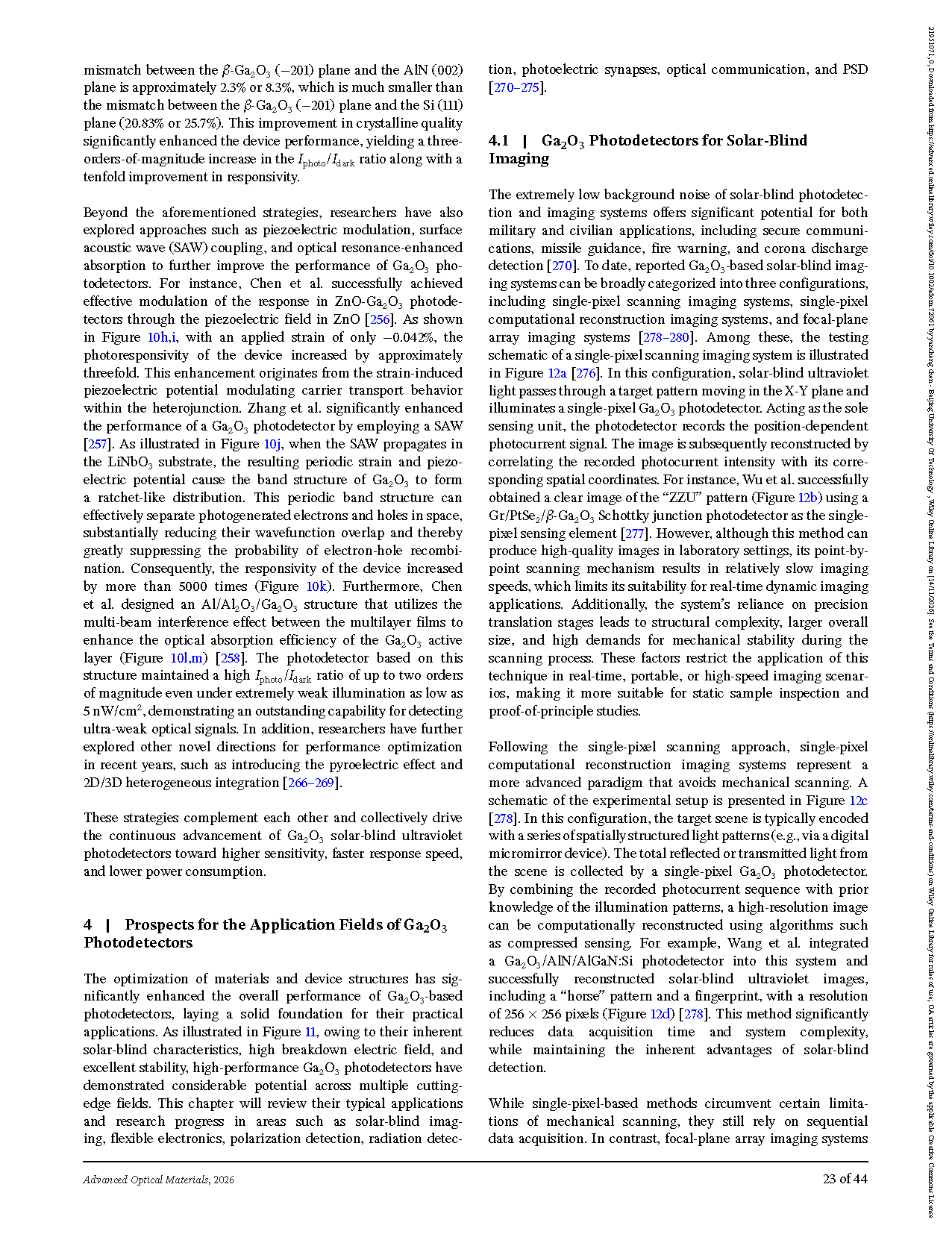
Application Prospects: From Solar-Blind Imaging to Intelligent Optoelectronic Systems
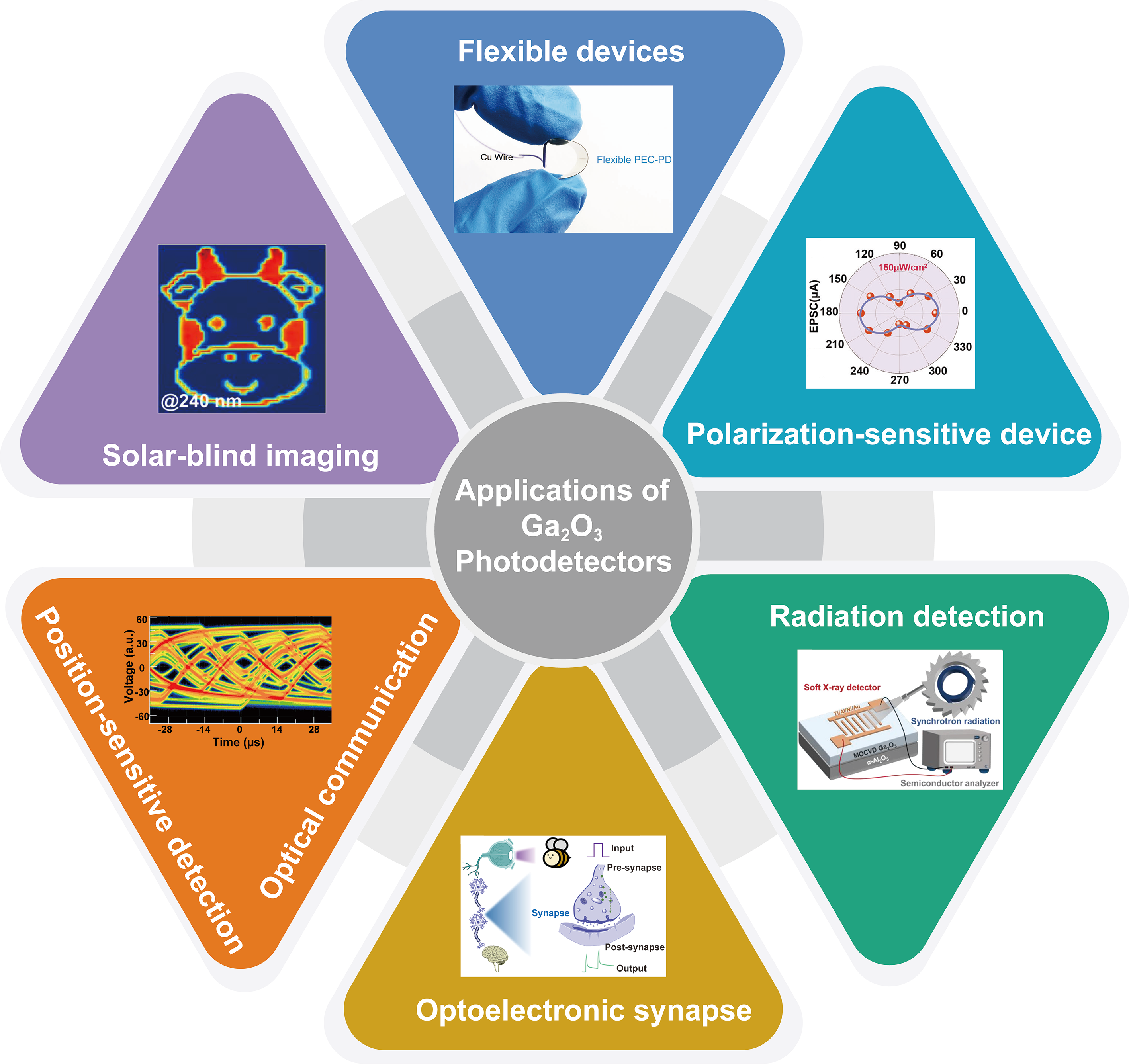
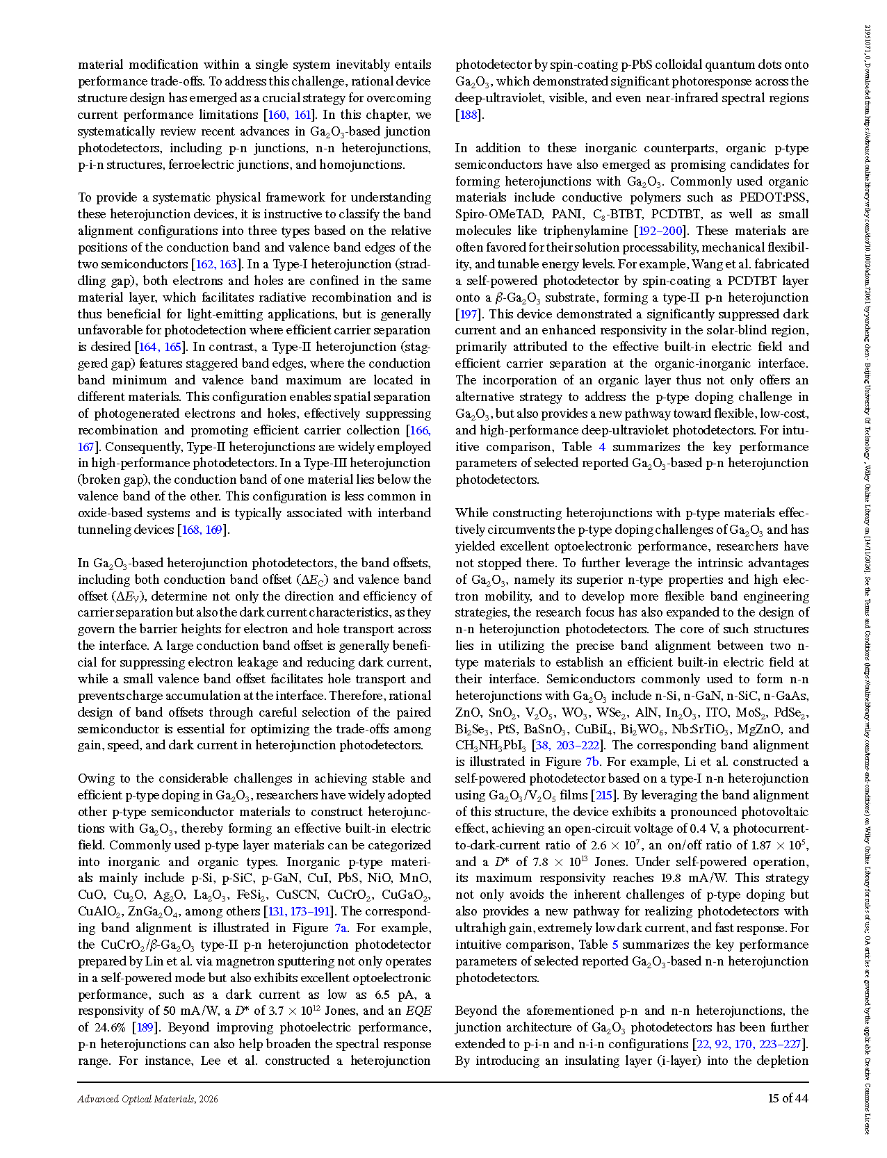
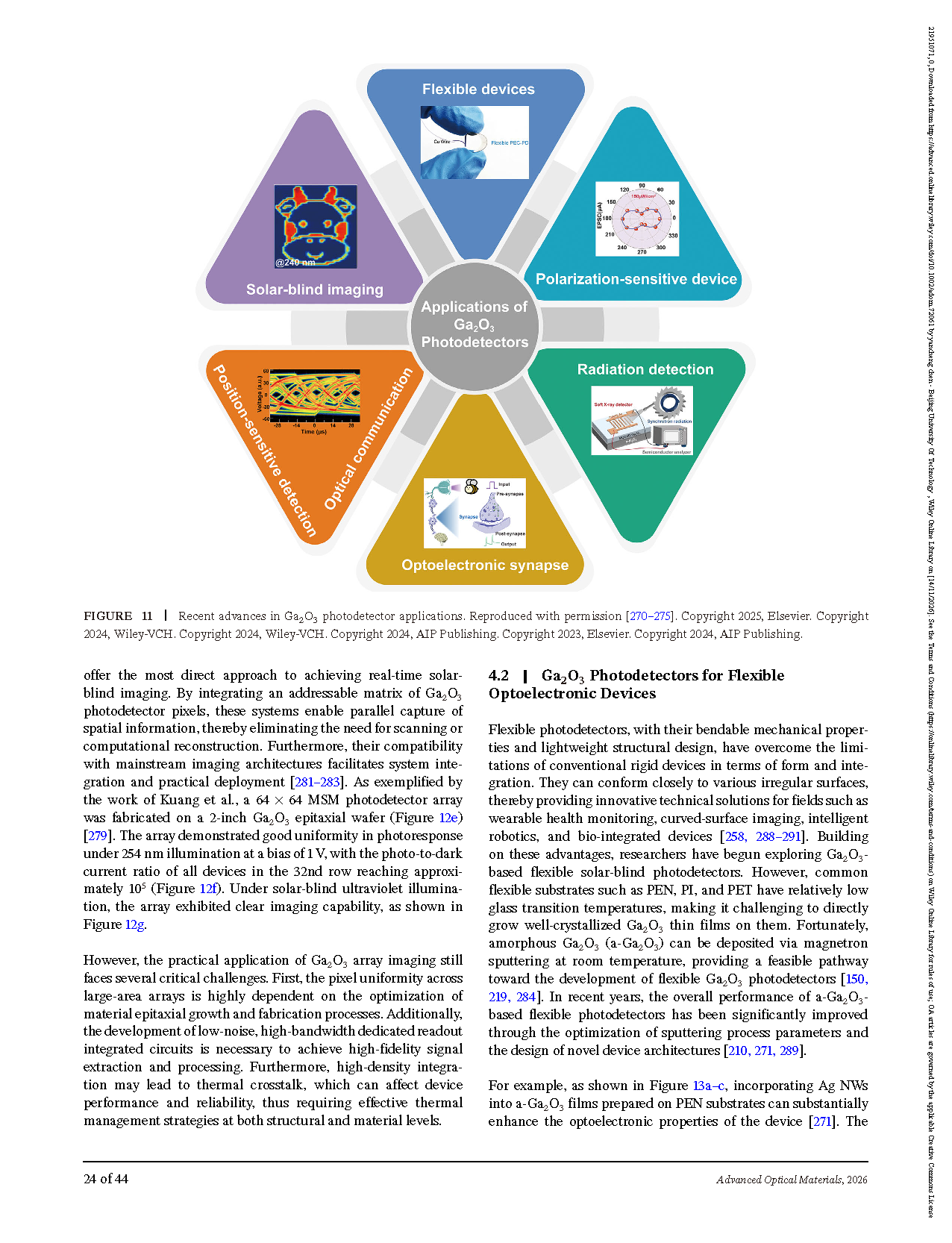
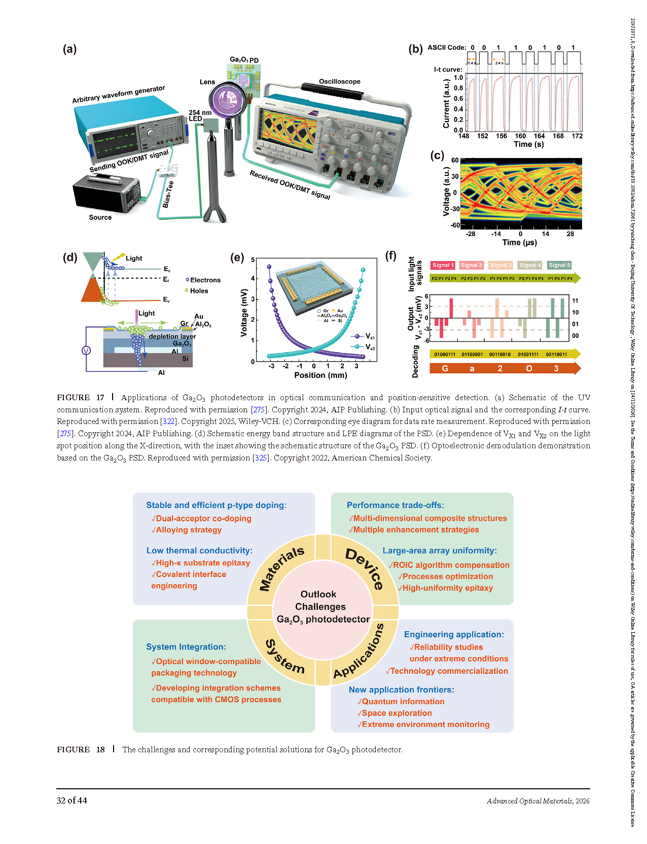
Fig. 4 Application exploration of Ga2O3 photodetectors.
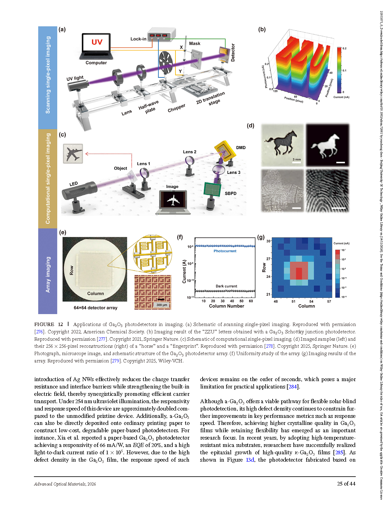
Solar-blind imaging: three technical routes—single-pixel scanning, single-pixel computational reconstruction, and focal plane arrays—are developing in parallel, and a 64×64 array has already demonstrated uniform imaging capability.
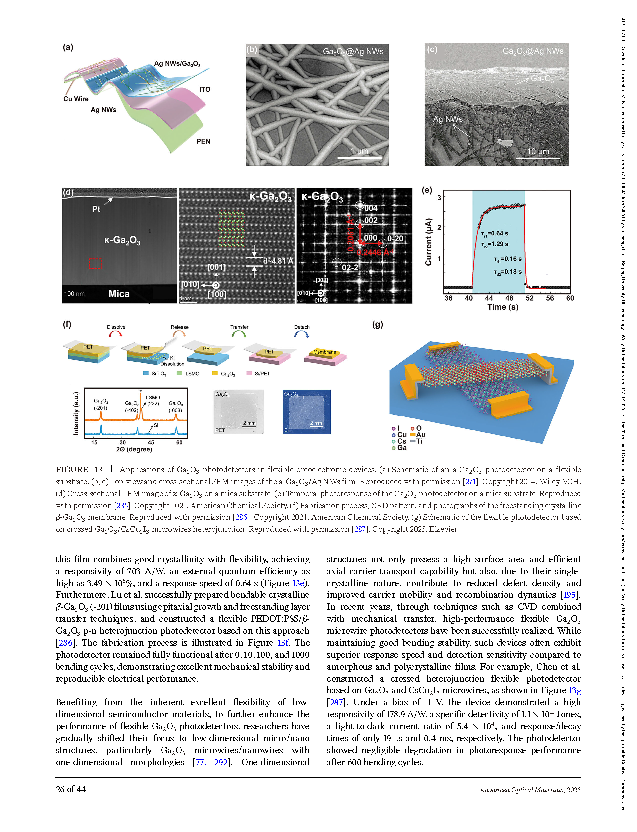
Flexible optoelectronics: approaches such as amorphous Ga2O3, κ-Ga2O3epitaxially grown on mica substrates, free-standing β-Ga2O3thin films, and microwire heterojunctions offer possibilities for wearable and curved-surface imaging.
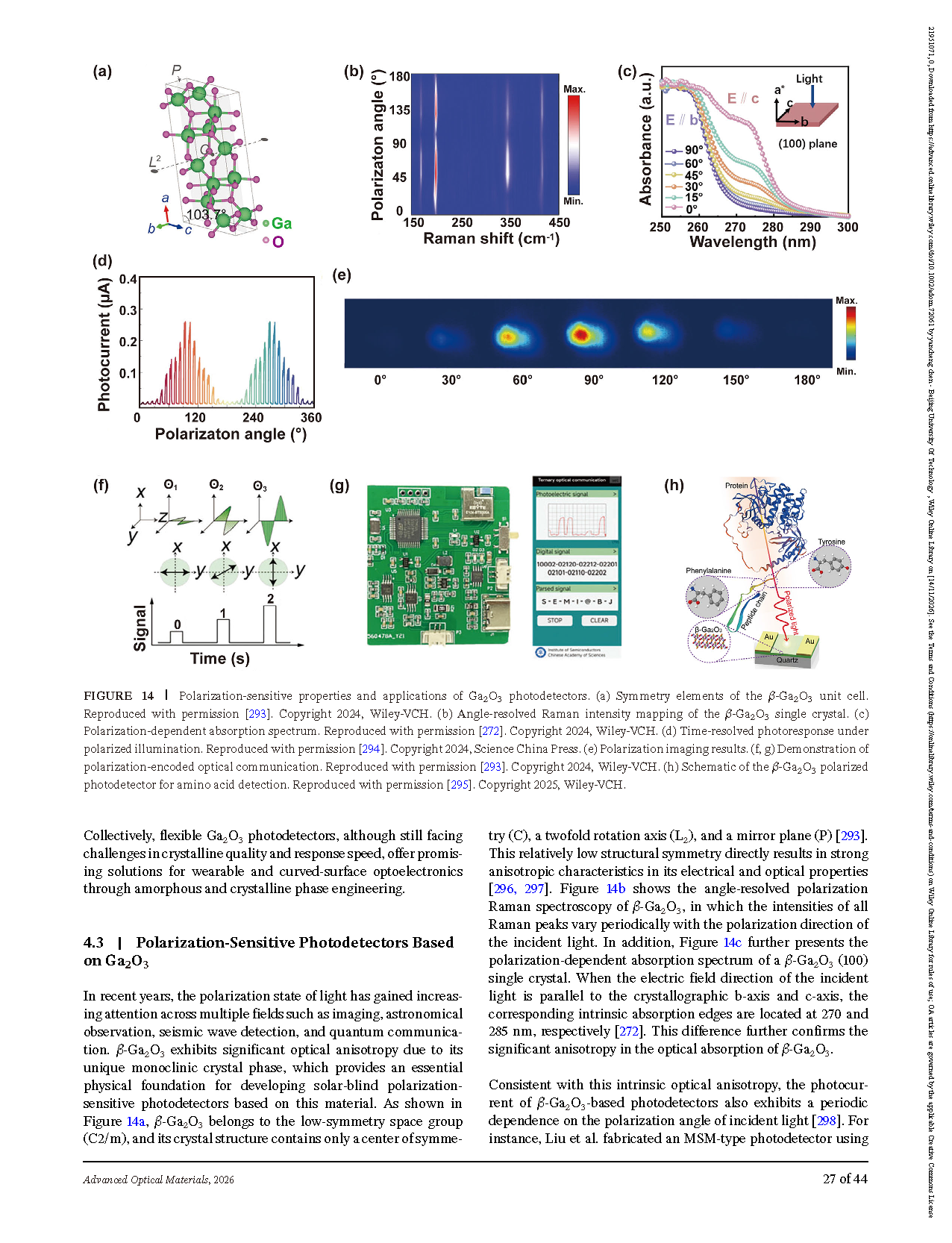
Polarization-sensitive detection: by exploiting the optical anisotropy of the monoclinic crystal system of β-Ga2O3, polarization imaging, polarization-encoded communication, and selective recognition of amino acids are realized.
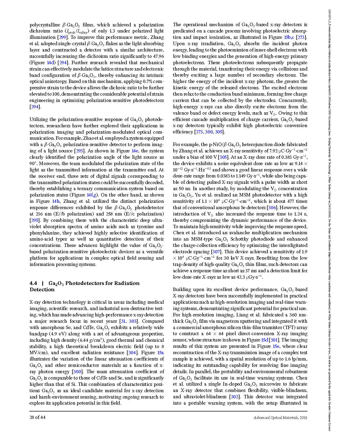
X-ray detection: owing to its high density, wide bandgap, and radiation resistance, Ga2O3shows potential in low-dose X-ray detection, high-resolution imaging, and portable warning systems.
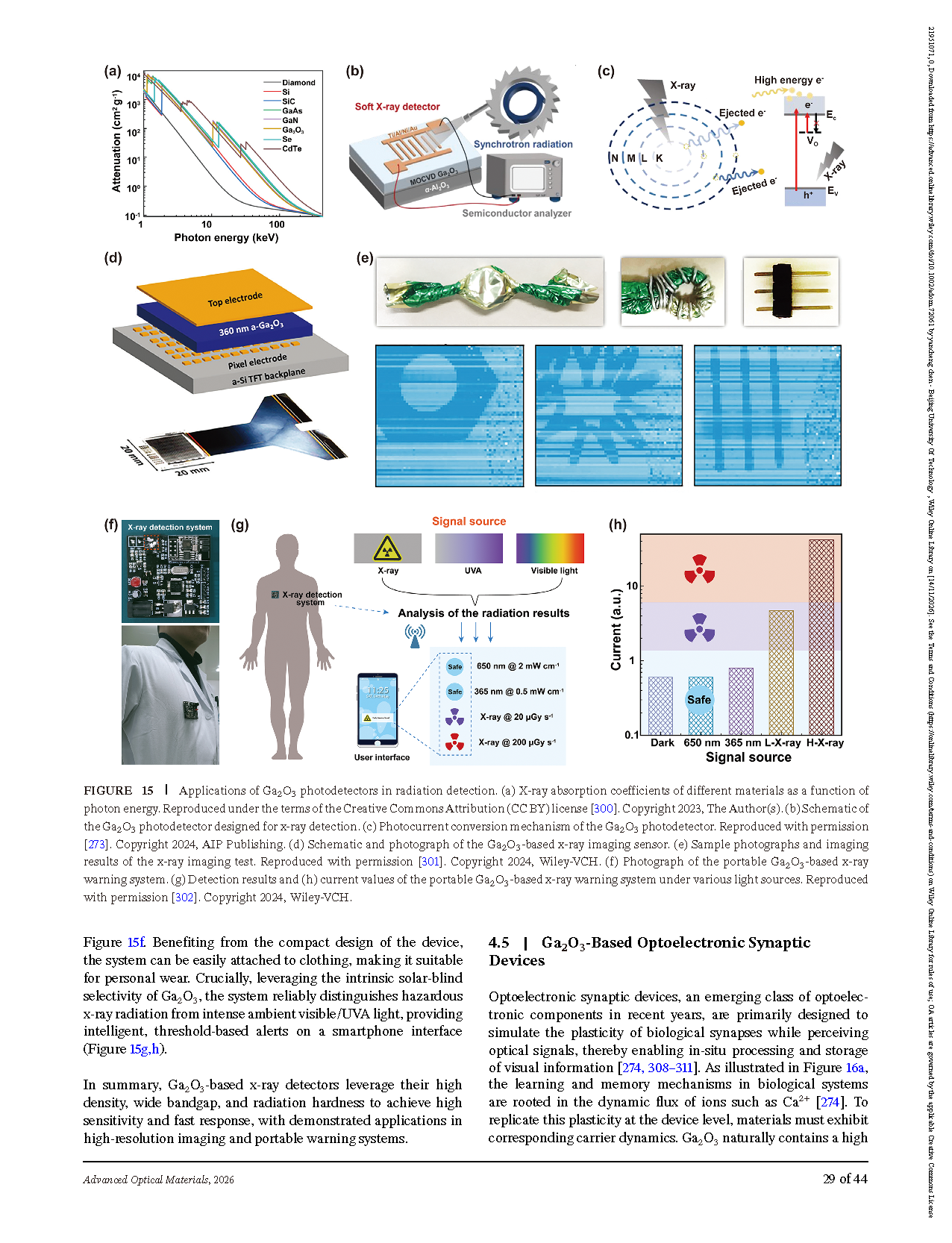
Optoelectronic synapses: oxygen-vacancy-related persistent photoconductivity is used to emulate synaptic plasticity, enabling the construction of artificial neural networks, logic gates, and information encryption systems.
Ultraviolet communication: Ga2O3photodetectors serve as receiving units to achieve high-signal-to-noise-ratio, anti-interference decoding of solar-blind ultraviolet signals.
Position-sensitive detection: based on the lateral photovoltaic effect, real-time monitoring of light spot position, angle, and displacement is achieved.
Challenges and Outlook: p-Type Doping, Thermal Conductivity, Performance Trade-offs, and System Integration
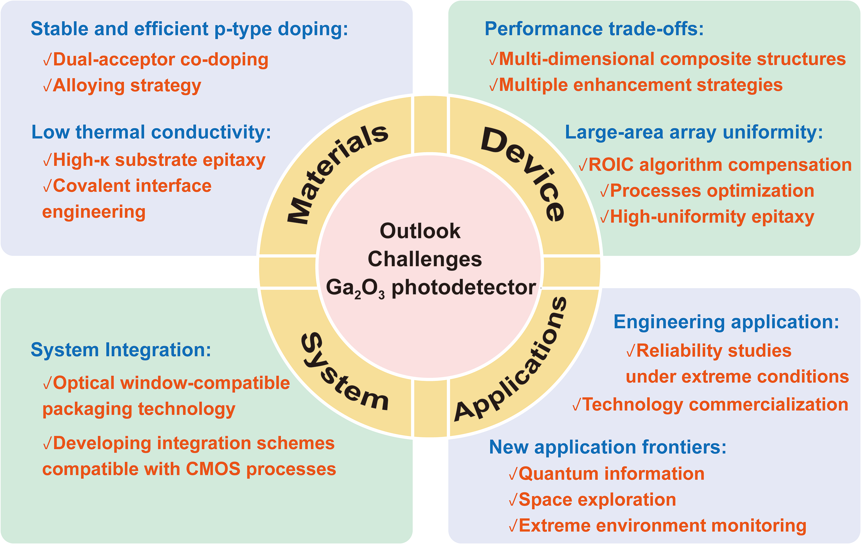
Fig. 5 Challenges of Ga2O3 photodetectors.
The article also identifies the bottlenecks in the field: stable and efficient p-type doping of Ga2O3 remains one of the greatest challenges; low thermal conductivity limits high-power and high-throughput detection; high gain, fast response, low dark current, and self-powered operation often constrain one another; and the uniformity of large-area arrays, CMOS-compatible packaging, long-term reliability, and cost/yield still need to be breakthroughs. In the future, multidimensional heterostructures, gradient bandgap design, synergy between local fields and heterojunctions, and heterogeneous integration with silicon-based readout circuits may become key pathways toward high-performance, low-power, intelligent deep-ultraviolet optoelectronic systems.
This review not only answers “how Ga2O3 solar-blind photodetectors can be made better,” but also systematically demonstrates “what they can be used for and what is still lacking.” For researchers engaged in wide-bandgap semiconductors, ultraviolet detection, flexible optoelectronics, and intelligent sensing, this is a field roadmap worth keeping.
DOI:
doi.org/10.1002/adom.72061
Instruction
Official Account

Cooperation
Top