Paper Sharing
【International Papers】Analysis of single event effects by heavy ion irradiation of Ga₂O₃ metal–oxide–semiconductor field-effect transistors
日期:2023-05-19阅读:1072
Researchers from the State Key Discipline Laboratory of Wide Band Gap Semiconductor Technology at Xidian University and Shaanxi Joint Key Laboratory of Graphene, School of Microelectronics have published a dissertation titled "Analysis of single event effects by heavy ion irradiation of Ga2O3 metal–oxide–semiconductor field-effect transistors" in the Journal of Applied Physics.
ABSTRACT
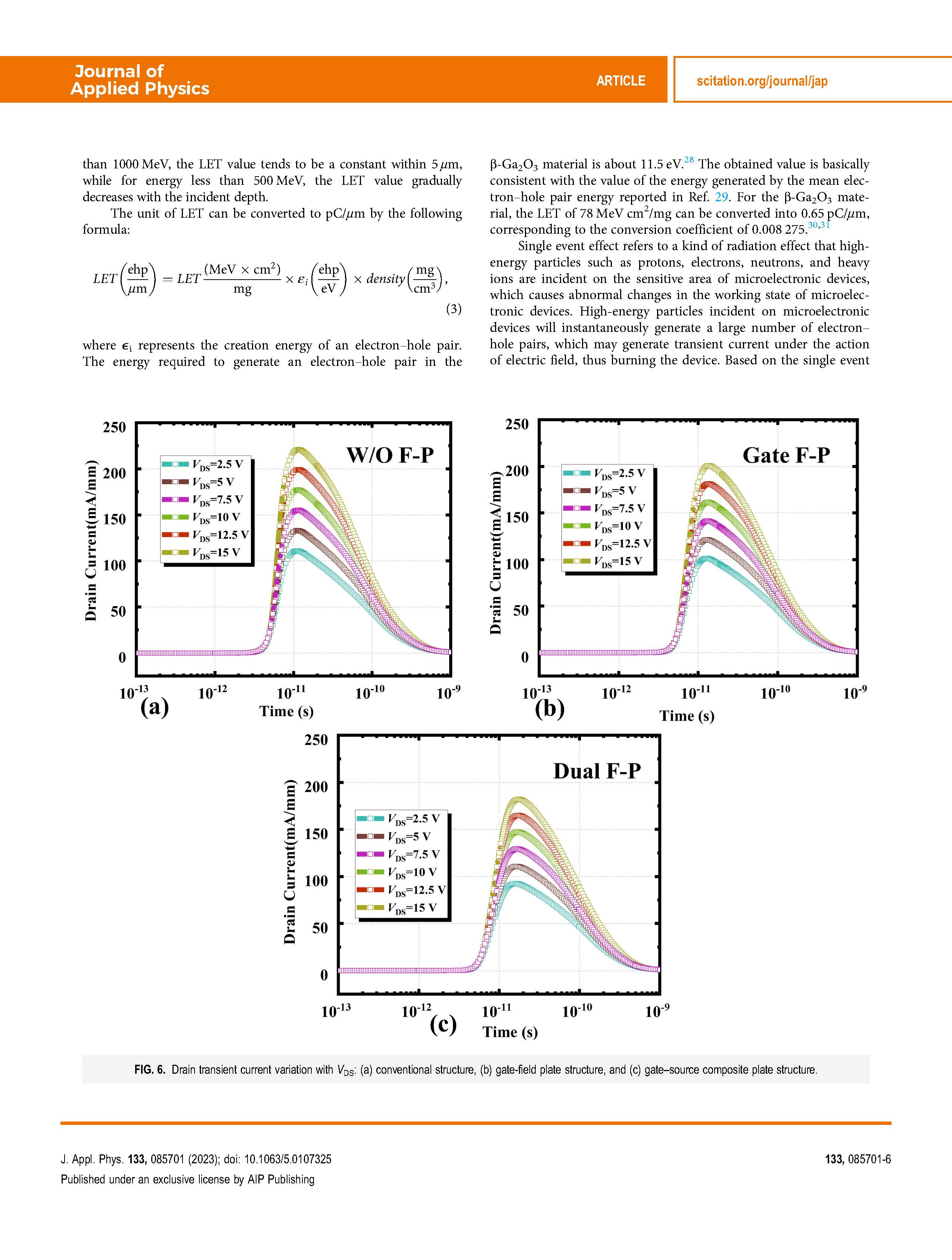
The model of lateral β-Ga2O3 metal–oxide–semiconductor field-effect transistor (MOSFET) was established using Sentaurus Technology Computer Aided Design software. The gate-to-drain distance of the device was 13.7 μm, and the breakdown voltage was 1135 V. The single event effect simulation model caused by heavy ion irradiation was introduced, and the effects of heavy ions’ incident position, angle, drain bias voltage, and linear energy transfer on the single event effect were studied. It is found that x=7.7 μm is the sensitive location of the single event effect at the gate corner near the drain side and the peak value of the transient current is 177 mA/mm. The effect of the terminal structure of the field plate on the transient effect of the single event effect of β-Ga2O3 MOSFET is studied. It is also found that the sensitive position of the single event effect of the conventional structure, gate-field plate structure, and gate–source composite field plate structure is around x=7.7 μm when VDS =10 V. The peak transient currents obtained are 177, 161, and 148 mA/mm. The single event effect pulse current of the three structures increases with an increase in the drain bias voltage, while the peak pulse current of the conventional structure is larger than that of the gate-field plate structure and the gate–source composite structure. The research shows that the terminal structure of the field plate is reliable means to reduce the single particle effect.

FIG. 1. β-Ga2O3 MOSFET device structure diagram: (a) conventional structure, (b) gate-field plate structure, and (c) gate–source composite field plate structure.

FIG. 2. (a) Simulated transfer characteristic of the Ga2O3 MOSFET; (b) simulated output characteristic of the Ga2O3 MOSFET.
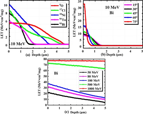
FIG. 3. LET variation with heavy ion incident depth: (a) different heavy ions, (b) Bi ions with different incident angles, and (c) Bi ions with different energies.
Paper sharing