


News Trends
【Industry News】Setting Sail, Gallium Oxide
日期:2023-06-02阅读:1133
Bypass Moore's Law, Researchers in Chinese Academy of Sciences Explore Semiconductor "Hybrid Rice" Technology
At present, the integrated circuit mainly uses silicon as the substrate material. However, compared with silicon, indium phosphate (InP), gallium nitride (GaN), gallium oxide (Ga₂O₃) and other compound semiconductors have a richer band structure and better electrical and optical properties. At the same time, the silicon material has approached the physical limit, and if the compound semiconductor and silicon are combined, the microelectronic device performance can be further promoted on the basis of maintaining the original device and process size.
Semiconductor heterointegration technology is to integrate compound semiconductor high-performance devices or chips of different process nodes with silicon-based low-cost high-integrated device chips through heterobond synthesis or epitaxial growth. This compound semiconductor heterointegration technology is similar to hybrid rice, which means to combine materials with different functions,and complement their advantages. The heterogeneous material interface can produce better electrical, optical, acoustic and thermal physical characteristics, and can achieve higher power, higher frequency and higher speed photon and electronic devices.
Shanghai Institute of Microsystems of Chinese Academy of Sciences has always been focusing on high-end silicon-based materials and applications. In the mid-1980s, research of silicone on insulator (SOI)materials was carried out. In the new century, SOI materials have been industrialized, filling the domestic gap. The SOI resembles a sandwich structure, introducing a layer of silica between the top silicon and the underlying silicon substrate.
In addition to high-quality silicon-based indium phosphide heterointegration, they are also working on highly thermal conductivity gallium oxide heterointegrated wafers. Gallium oxide is considered to be the most promising wide band gap semiconductor material to achieve industrial application after gallium nitride and silicon carbide. It has application prospects in the field of power devices, but its fatal defects are low thermal conductivity and poor heat dissipation ability, which affect the life of devices. Since 2018, the research team headed by You Tiangui explore to integrate the gallium oxide with substrate,which has high thermal conductivity, to help dissipate its heat. They realized the heterogeneous integration of wafer level gallium oxide single crystal film and high thermal conductivity substrate (Si or SiC) for the first time by using ion beam stripping and transfer technology, which increases 4 times heat dissipation capacity of gallium oxide power device, solving the bottleneck problem of the gallium oxide device heat dissipation.
The research team headed by You Tiangui is also exploring to solve the process problem of high thermal conductivity gallium oxide heterointegrated wafer. Ion beam stripping and transfer technology are used to "stick" the two materials together. Due to the different thermal expansion coefficient of the material, the temperature increases, the material expands, and the stress generation is easy to destroy the heterointegrated materials. For this reason, the materials must be closely fitted. Different from the Japanese bonding technology in the past, in order to realize autonomous control, You Tiangui research team developed thermal bonding technology, which reduces stress and does not need to operate in a vacuum environment, and is more suitable for mass production.
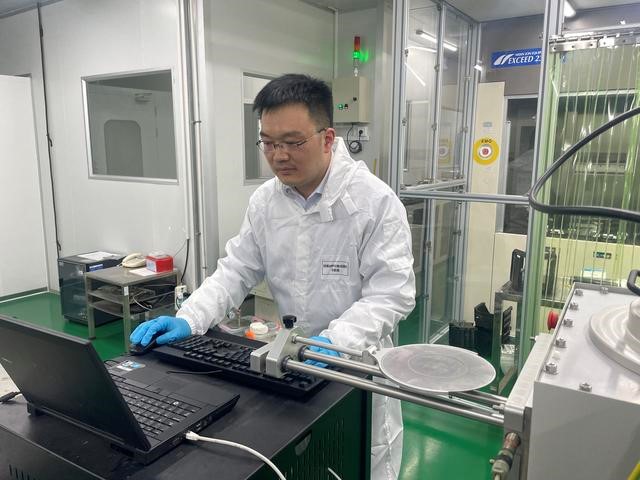
The key laboratory of our university has successfully prepared high-voltage-withstand performance semiconductor materials
Recently, Professor Chen Haifeng's team from the Key Laboratory of New Semiconductor Devices and Materials, managed by the School of Electronic Engineering in our university, successfully prepared high-quality gallium oxide epitaxial wafers on 8-inch silicon wafers, which marks an important progress in the research of ultra-wide band gap semiconductor in our university.
Professor Chen Haifeng, the team leader, introduced that gallium oxide is an ultra-wide band gap semiconductor material, with excellent high voltage withstand and solar blind ultraviolet light response characteristics, and has great potential in the field of power devices and optoelectronics. Gallium oxide heteroepitaxy on silicon is conducive to the direct integration of silicon circuit and gallium oxide circuit, and has the advantages of low cost and good heat dissipation.
The Key Laboratory of New Semiconductor Devices and Materials has invited Hao Yue, academician of Chinese Academy of Sciences and scientist of microelectronics and solid electronics, as the chief scientist. The team has more than 30 teachers and students. It has a complete gallium oxide process experimental line and ultra-clean process room, mainly studying ultra-wide band gap gallium oxide materials and devices. The team has rich scientific research experience in gallium oxide material growth, device preparation, testing and characterization. And it is undertaking many research projects funded by the National Natural Science Foundation of China, Shaanxi Natural Science Foundation of Shaanxi Province and Shaanxi Provincial Department of Education. Over 100 research papers published in Physics, Semiconductor, IEEE Electron Device Letters, Journal of Applied Physics, IEEE Transactions on Electron Devices, Physics Letters A, Nanotechnology, Applied Surface Science, Carbon, and has been authorized more than 20 national invention patents.
Cultivating in the Spring of Artificial Crystals
Compared with two years ago, when entering the company exhibition hall to introduce for the reporter, Zhang Xuefeng was more joyful, because the new research and development project that he has been brewing for a long time has been substantially promoted.
The new project is the research and industrialization of the fourth generation semiconductor material gallium oxide single crystal material, which is included in the key research and development plan in Ningxia province in 2022. The project is an aim that Zhang Xuefeng gave himself several years ago. He hopes to solve various problems encountered in the research and development in his own way, rather than "copy homework".
Gallium oxide, a new type of ultra-wide band gap semiconductor material, is recognized the fourth generation of semiconductor materials around the world. Compared with the third generation semiconductor materials such as silicon carbide and gallium nitride, gallium oxide has lower cost and better performance, and has great application value in key fields such as ultra-high voltage transmission, high-speed railway, aerospace and military weapons. Although gallium oxide is still in the research and development stage, but the semiconductor companies are competing to layout.
"The current situation is that the production cost at home and abroad is very high, the price of 4-inch gallium oxide wafer is between 40,000 yuan and 60,000 yuan, such a price is almost impossible to be used in the civil industry. I want to solve this problem of low production efficiency and high production cost through our own technology, so that gallium oxide wafer can be used in the civil industry, and the products can be affordable for ordinary people." Zhang Xuefeng said.
It is not easy for a R & D project to shift from a laboratory to industrialization. There are numerous challenges at the technical level, as well as unexpected market risks. But, Zhang Xuefeng decided to take the plunge. Since Zhang Xuefeng's company is an innovative small and micro enterprise, it is difficult to apply for bank loans for production expanding. In order to fight for investment, Zhang Xuefeng has moved south several times in recent months and is currently in cooperation negotiations. In addition, Zhengzhou University also offered an olive branch to him. After preparation, the two sides plan to set up a joint research institute in April this year to jointly draw the blueprint for the research and industrialization of gallium semiconductor material gallium oxide.

Shanxi Huaxin Semiconductor Industrial Base Project (phase II) is expected to be fully completed and put into operation by the end of this year
According to the official micro information of Shanxi Comprehensive Reform Demonstration Zone, recently, the main project of workshop of Shanxi Huaxin Semiconductor Industrial Base Project (phase II) has started construction, and it is expected that by the end of 2023, the project will be fully completed and put into operation.

It is reported that Shanxi Huaxin Semiconductor Industrial Base is a major strategic layout of Qingdao Golden Star Electronics Technology Co., Ltd. in the semiconductor industry, with a total investment of 552 million yuan. At present, the first phase of the project has been started, put into production and regulated in 2022. After the second phase of the project is fully completed and put into operation, it will layout the large size sapphire growth, large size indium hite crystal growth and processing, military large size transparent armor single crystal production and development, gallium oxide crystal development and growth and crystal processing projects, so as to achieve full coverage of middle and high-end semiconductor compound materials.
Meng Fanqi, head of the base, said that Shanxi Huaxin Semiconductor Industry Base will actively introduce upstream and downstream enterprises, such as equipment, chip packaging enterprises, to jointly build a domestic advanced semiconductor industry cluster.
