


News Trends
【Domestic News】Luo Xiaorong research team has made progress in the field of ultra-wide band gap semiconductor gallium oxide device in Power Integration Technology Laboratory in UESTC (University of Electronic Science and Technology of China)
日期:2023-07-21阅读:1162
Semiconductor material gallium oxide has become the focus and heat spot of research at home and abroad, due to its large band width and high critical breakdown electric field, with its Baliga’s figure of merit is 3444 times more than Si, and it can grow high quality, large size of single crystal through a variety of lower cost melt method. It can meet a new generation of power system and power electronic device needs for high power, high efficiency and miniaturization development. It is clearly listed as an export control by a certain country. Recently, China also implements export control on gallium and germanium and related items, which has become a hot spot and focus of research at home and abroad. In recent years, led by professor Zhang Bo from the Institute of Integrated Circuit, professor Luo Xiaorong’s team in Power Integration Technology Laboratory started the research on ultra-wide band gap gallium oxide devices, and made a series of new progress in the new gallium oxide power rectifier tube and transistor and its reliability research, and have published several papers on some international authoritative journals and top conference in this field, and a number of patents authorized.

1、gallium oxide power devices
In view of the technical difficulties that the breakdown voltage of gallium oxide power devices is far below the theoretical limit and it is difficult to achieve enhanced devices, the project team proposed four new structures to improve the breakdown voltage strength of the rectifier and reduce the opening voltage, increase the transistor threshold voltage and reduce the reverse conduction voltage. The team developed a gallium oxide Schottky barrier diode with a composite structure of air bridge field plate and thermal oxidation terminal composite structure, whose breakdown voltage increases by 176% compared with the device without the composite terminal structure, and the reverse recovery time decreases by 25% and 81% compared with the commercial SiC and Si diodes, respectively. The team developed a gallium oxide junction barrier Schottky diode with NiO / gallium oxide heterojunction and field plate(FP JBSD)[7],whose forward I-V, C-V characteristics and the breakdown voltage were almost unchanged before and after the high-temperature stress at 3000 min. The team proposed a FOCF diode with a Fin trench, an Ohm contact anode, and a composite field plate, achieving 0.45V low open voltage. The team also integrated the gallium oxide diode with FinFET, allowing the threshold voltage and reverse conduction voltage to be controlled separately, obtaining an enhanced gallium oxide RC-FinFET [3] with low reverse conduction voltage of 0.45V and high threshold voltage of 1.6V, enhancing its potential in high power and low loss power conversion systems.

Figure 1 CT SBD and contrast structure (a) comparison of withstand voltage test and (b) comparison of reverse recovery characteristics

Figure 2 FP JBSD Forward I-V characteristics before and after high temperature stress
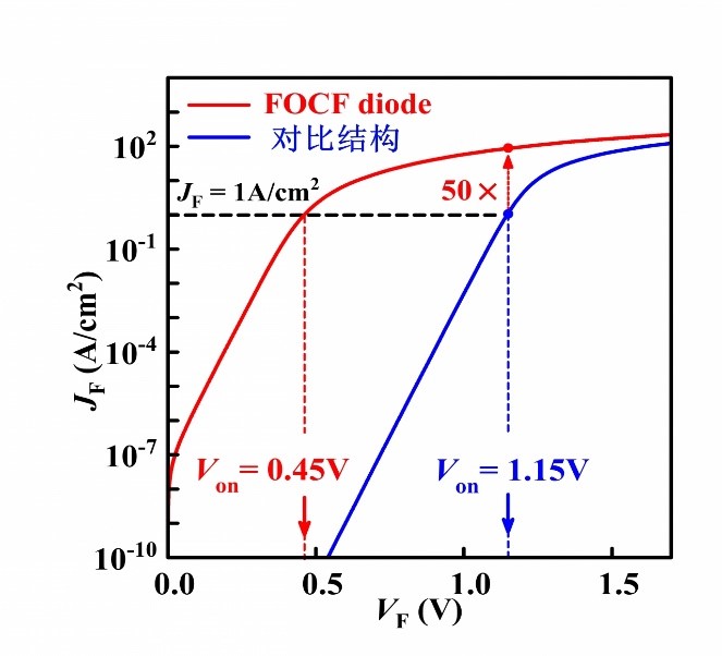
Figure 3 Forward I-V properties of the FOCF diode and contrast structures
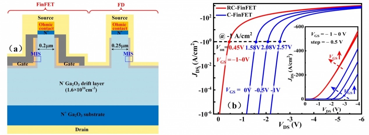
Figure 4 (a) Schematic diagram of RC-FinFET and (b) Comparison of reverse conduction performance of RC-FinFET and C-FinFET
2、FETs reliability of gallium oxide
Ultra-wide band gap gallium oxide devices are expected to work in extreme environments such as high power and high temperature, so studying the defect response mechanism of gallium oxide devices in multiple physical fields such as electric and thermal fields is crucial to promote their application. The team systematically analyzed the instability of gallium oxide MOSFET under electric-thermal stress, and revealed the degradation mechanism and physical model under the electric field and thermal field.The positive bias stress was found to cause boundary traps in the oxide layer to trap electrons, leading to a forward drift of the VGS-IDS curve. As the ambient temperature increases, hysteresis analysis found that the deep main interface state is gradually activated and involved in the trapping process, together with the boundary trap, the device causes a more severe VGS-IDS curve drift [4]. Unlike the positive bias stress, the boundary trap, interface state and body trap under normal temperature and negative bias stress together lead to the degradation of gallium oxide MOSFET performance. The ionization trap model proposed by the team explains the non-unified mechanism under positive / negative bias stress, and then the accuracy of the model is verified by simulation [5]. The team studied the degradation mechanism of NiO / β-gallium oxide heterogate FET under different stress voltages and stress times, and found that there are two different degradation mechanisms operating under negative bias stress, which provides theoretical guidance for the development of reliability reinforcement techniques for NiO / β-Ga2O3 heterojunction devices [6].

Figure 5 Ga2O3 MOSFET (a)VGS-IDS curve under positive bias stress under normal temperature; (b) hysteresis led by the main interface state’s being activated with temperature rise and (c) VGS-IDS curve under positive bias stress of 125℃

Figure 6 Ga2O3 MOSFET(a) Changes in the three trap density under positive / negative bias stress; the VGS-IDS curves for the experiment and simulation are fitted under (b) positive / (c) negative bias stress

Figure 7 NiO / β-Ga2O3 heterojunction gate FET(a) the VGS-IDS curve under the negative bias stress; (b) extracted VTH and VGS-IGS curves
Since formed in 2021, Professor Luo Xiaorong’s team led and participated in two key projects of the national science and technology plan, among which, the University of Electronic Science and Technology as the lead unit, Luo Xiaorong as the technology chief, in close cooperation with domestic first-class teams in the field of ultra-wide band gap semiconductor gallium oxide materials and devices, such as the 13th Research Institute of CLP Group, Xidian University, University of Science and Technology of China and other units. The project has made a series of important progress.
original links:
[1] https://ieeexplore.ieee.org/document/9392264
[2] https://ieeexplore.ieee.org/document/9975152
[3] https://ieeexplore.ieee.org/document/10130497
[4] https://ieeexplore.ieee.org/document/9831113
[5] https://ieeexplore.ieee.org/document/9882012
[6] http://www.jos.ac.cn/en/article/id/b242a0ef-b389-4569-b50d-cc004066034c
