


Member News
【Member News】New research by Professor Han Genquan, Xidian University: Heterointegration technology realizes thermal management of gallium oxide electronic devices
日期:2023-07-31阅读:1024
The more severe phonon-phonon scattering in gallium oxide (Ga2O3) crystals leads to a lower thermal conductivity than in most other semiconductor materials. To solve this problem and improve the heat dissipation capability of Ga2O3 devices, a practical and effective solution is to integrate Ga2O3 with a substrate with high thermal conductivity. Professor Han Genquan of Xidian University published an article titled "Heterogeneous Integrated Technology Realizes Thermal Management of Ga2O3 electronic devices" in issue 6 of Semiconductor Journal 2023. In the article, the research team conducted in-depth research on existing thermal management solutions for Ga2O3 electronic devices, and the authors show that the successful development of ion-cutting and bonding processes enables whole-chip-level heterogeneous integration on silicon carbide (SiC) and silicon (Si) substrates. Using these substrates with high thermal conductivity and good insulation properties, heterointegrated Ga2O3 transistor devices show improvements in temperature-dependent open-and off-state current performance relative to block material devices. Experiments demonstrate that during ion cutting, the effect that hydrogen ion injection had on Ga2O3-transistor trenches can be eliminated by high-temperature annealing, thus making the effective trench mobility of heterointegrated Ga2O3 transistors comparable to bulk materials and bulk devices. Heterointegration technologies are expected to address the fundamental thermal limitations of Ga2O3 electronic devices in high-power applications.
Full Text
The more severe phonon−phonon scattering in gallium oxide (Ga2O3) crystals leads to lower thermal conductivity compared to most other semiconductor materials. To address this issue and enhance the heat dissipation in Ga2O3 devices, one practical solution is to integrate Ga2O3 with a highly thermally conductive substrate, such as SiC and Si. Currently, there are three methods employed for the heterogeneous integration of Ga2O3 with highly thermally conductive substrates: mechanical exfoliation, hetero-epitaxy growth, and ion-cutting technique.
Mechanical exfoliation involves splitting Ga2O3 thin flakes with a thickness ranging from 20 to 400 nm from the bulk Ga2O3 due to its large lattice constant along the [100] direction[1]. These exfoliated thin flakes can be integrated heterogeneously onto any substrate using van der Waals interaction. The thin flakes retain good crystal quality and a smooth interface similar to bulk Ga2O3 due to the lossless transfer process. However, mechanical exfoliation is not suitable for wafer-scale manufacturing as it can only fabricate thin flakes of around a few micrometers in size with uncontrollable thickness and uniformity. Moreover, the weak intermolecular forces between Ga2O3 thin flakes and the substrate hinder the heat transport across the heterogeneous interface[2].
The direct growth of Ga2O3 thin films on highly thermally conductive substrates provides more flexibility. Various epitaxy methods such as molecular beam epitaxy (MBE), low-pressure chemical vapor deposition (LPCVD), and pulsed laser deposition (PLD) have been used to grow high-quality Ga2O3 thin films on these substrates. However, the hetero-epitaxially grown Ga2O3 thin films have a higher full-width at half-maximum (FWHM) of 558 arcsec in the X-ray diffraction (XRD) rocking curves compared to homoepitaxial Ga2O3 thin films[3]. Lattice mismatch and substrate oxidation during the epitaxy process are key issues that need to be addressed.
The ion-cutting technique has proven to be an elegant method for heterogeneous integration. It involves splitting a high-quality wafer-scale thin film from a bulk wafer through hydrogen (H) or/and helium (He) ion implantation, creating a damage layer below the wafer surface. The sliced thin film is then transferred onto a handle wafer via a wafer bonding process, as shown in Fig. 1[4]. The exfoliated wafer-scale thin film maintains good crystallization quality similar to the donor bulk, and the remaining bulk can be recycled to lower the process cost. Ga2O3, being an ultra-wide bandgap semiconductor, is particularly suitable for the ion-cutting technique as it efficiently extracts heat from its active layer to the highly thermally conductive substrate. In 2019, we first realized a wafer-scale single-crystalline Ga2O3 thin film heterogeneously integrated onto high thermal conductivity substrates (Si and SiC) using the ion-cutting technique with H implantation and surface-activated bonding process. The resulting wafer had a size of 2 inches with a Ga2O3 thickness nonuniformity of less than 2%. A post-annealing process at 900 °C for 30 min resulted in an FWHM of 90 arcsec in the XRD rocking curves, which is very close to that of the donor bulk Ga2O3.

Fig. 1. The process flow for transferring β-Ga2O3 thin film onto SiC (or Si) by ion-cutting. Reprinted from Xu et al.[4]. Copyright 2021, with permission from IEEE.
The difficulty in splitting Ga2O3 thin films arises from the low utilization ratio of H ions, which is around 9%, and the large activation energy of 2.28 eV in bulk Ga2O3. This necessitates a much higher implantation fluence compared to other materials. Regarding wafer bonding, two different methods are employed: surface activated bonding (SAB) and hydrophilic bonding. SAB enables the achievement of a strong bonding strength at room temperature without the need for wet chemical cleaning. However, SAB involves a sputtering process that can negatively impact the crystallinity of the thin film surface and further degrade the thermal and electrical properties at the heterogeneous interface. An alternative approach is hydrophilic bonding, which occurs at an elevated temperature. This method minimizes significant damage to the wafer surfaces and helps resist thermal stress during the exfoliation process. By employing hydrophilic bonding, a 2-inch Ga2O3 thin film was successfully transferred onto a SiC substrate[5].
The heterogeneous integration of Ga2O3 with a highly thermally conductive substrate leads to a significant improvement in thermal dissipation for Ga2O3 devices. When compared to Ga2O3 bulk wafers, Ga2O3/SiC heterostructures exhibit a much faster thermal relaxation speed. Lateral Schottky barrier diodes fabricated on Ga2O3-on-SiC (GaOSiC) heterogeneous wafers also demonstrate improved thermal dissipation compared to those on Ga2O3 bulk. The high thermal conductivity of the SiC substrate allows GaOSiC SBDs to reach a peak rising temperature that is only one quarter of that observed on Ga2O3 bulk when subjected to the same applied power[6]. The heterogeneous integration of Ga2O3 on SiC or Si not only improves the thermal dissipation properties of the devices but also provides effective insulating substrates[7, 8]. In heterogeneous Ga2O3 metal−oxide−semiconductor field-effect transistors (MOSFETs), the OFF-state leakage current only increases by 1−2 orders of magnitude as the ambient temperature rises from room temperature to approximately 250 °C. In contrast, the OFF-state leakage current of Ga2O3 bulk devices degrades by 5−6 orders under the same conditions. It is important to note that the ideal insulating Ga2O3 is not yet available. Semi-insulating Ga2O3 can be achieved through high concentration Fe compensation doping, but this introduces n-type conductivity in the Ga2O3 substrate as the temperature increases.
The effective channel mobility (μeff) is a critical factor that influences the drive current of transistors and serves as an important measure of the quality of Ga2O3 films in heterogeneous integration. It has been observed that the μeff of heterogeneous Ga2O3 MOSFETs on SiC and Si substrates can be enhanced by increasing the post-annealing temperature of the Ga2O3 channel[7, 9]. In particular, when the GaOSiC transistor is annealed at 1200 °C, the μeff achieved is consistent with that of the Ga2O3 donor wafer used for fabricating the GaOSiC wafer, as well as reported bulk Ga2O3 materials and devices, as illustrated in Fig. 2. This indicates that the defects induced into the Ga2O3 channel during the ion-cutting process can be effectively eliminated through high-temperature annealing.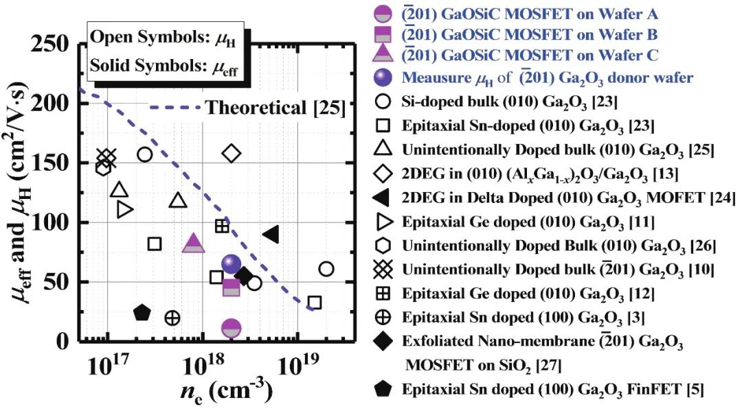
Fig. 2. Benchmarking the measured μeff of GaOSiC MOSFETs against the reported Hall mobility and μeff of bulk β-Ga2O3 materials and devices (data from Ref. [7] and references therein). Reprinted from Wang et al.[7]. Copyright 2021, with permission from IEEE.
The performance of recessed-gate GaOSiC MOSFETs has been demonstrated to be excellent[10]. For instance, a device with a gate-to-drain length (LSD) of 3 μm and a channel length (LCH) of 1 μm achieved a specific ON-resistance (RON,sp) as low as 0.72 mΩ·cm2, which is the lowest value during that time. Another recessed-gate transistor with an LSD of 11 μm achieved a breakdown voltage (Vbr) of 1000 V and an RON,sp of 100 mΩ·cm2, resulting in a power figure-of-merit (PFOM) of 100 MW/cm2. Notably, this PFOM value remained stable even with the ambient temperature ranging from 25 to 200 °C, as depicted in Fig. 3.
Fig. 3. Benchmarking RON,sp versus Vbr for the heterogeneous GaOSiC MOSFETs with the reported β-Ga2O3 transistors (data from Ref. [10] and references therein). Reprinted from Wang et al. [10]. Copyright 2022, with permission from IEEE.
Successful development of ion-cutting and bonding processes for Ga2O3 semiconductors has enabled the heterogeneous integration of wafer-scale β-Ga2O3 thin films onto 4H-SiC and Si (001) substrates. The utilization of these substrates with high thermal conductivity and good insulating properties has led to improved temperature-dependent ON- and OFF-state current performance in heterogeneous Ga2O3 MOSFETs compared to bulk devices. Experimental demonstrations have shown that the effects induced in the Ga2O3 channel by H+ implantation during the ion-cutting step can be eliminated through high-temperature annealing, resulting in comparable effective channel mobility (μeff) in heterogeneous Ga2O3 MOSFETs compared to bulk materials and transistors. Heterogeneous integration technology holds promise in overcoming the fundamental thermal limitations of Ga2O3 electronics for high-power applications.
References:
[1] Barman S K, Huda M N. Mechanism behind the easy exfoliation of Ga2O3 ultra-thin film along (100) surface. Phys Status Solidi RRL, 2019, 13, 1800554
[2] Cheng Z, Wheeler V D, Bai T Y, et al. Integration of polycrystalline Ga2O3 on diamond for thermal management. Appl Phys Lett, 2020, 116, 062105
[3] Li Z M, Jiao T, Yu J Q, et al. Single crystalline β-Ga2O3 homoepitaxial films grown by MOCVD. Vacuum, 2020, 178, 109440
[4] Xu W H, Wang Y B, You T G, et al. First demonstration of waferscale heterogeneous integration of Ga2O3 MOSFETs on SiC and Si substrates by ion-cutting process. 2019 IEEE International Electron Devices Meeting (IEDM). San Francisco, CA, USA. IEEE, 2020, 12.5. 1
[5] Shen Z H, Xu W H, Chen Y, et al. Wafer-scale single-crystalline β-Ga2O3 thin film on SiC substrate by ion-cutting technique with hydrophilic wafer bonding at elevated temperatures. Sci China Mater, 2023, 66, 756
[6] Xu W H, You T G, Wang Y B, et al. Efficient thermal dissipation in wafer-scale heterogeneous integration of single-crystalline β-Ga2O3 thin film on SiC. Fundam Res, 2021, 1, 691
[7] Wang Y B, Xu W H, Han G Q, et al. Channel properties of Ga2O3-on-SiC MOSFETs. IEEE Trans Electron Devices, 2021, 68, 1185
[8] Wang Y B, Xu W H, You T G, et al. β-Ga2O3 MOSFETs on the Si substrate fabricated by the ion-cutting process. Sci China Phys Mech Astron, 2020, 63, 277311
[9] Wang Y B, Xu W H, Han G Q, et al. Channel mobility properties of β-Ga2O3 MOSFETs on Si substrate fabricated by ion-cutting process. 2021 5th IEEE Electron Devices Technology & Manufacturing Conference (EDTM). Chengdu, China. IEEE, 2021, 1
[10] Wang Y B, Han G Q, Xu W H, et al. Recessed-gate Ga2O3-on-SiC MOSFETs demonstrating a stable power figure of merit of 100 mW/cm² up to 200 °C. IEEE Trans Electron Devices, 2022, 69, 1945
