


News Trends
【Domestic News】Gallium Oxide Epitaxial Growth and Power Devices(Ⅱ)
日期:2023-08-04阅读:1512
5、Rapid epitaxy of 2-inch and high-quality α-Ga2O3 films by Mist-CVD method
The gallium oxide (Ga2O3), as an ultra-wide band gap semiconductor material, has a broad application prospect in power devices, deep ultraviolet optical electrical parts, microwave devices and other fields in the future. The gallium oxide materials have five common crystalline phases, namely α, β, γ, ε, δ, among which, the metastable α-Ga2O3 shows a larger band width (5.3 eV), higher breakdown field strength (10 MV / cm) and better Baliga’s figure of merit (6276) in the gallium oxide material family, attracting wide attention in the industry in recent years. Currently, the methods used for preparing α-Ga2O3 mainly include Hydride Vapor Phase Epitaxy (HVPE), Metal-Organic Chemical Vapor Deposition (MOCVD), Molecular Beam Epitaxy (MBE), and Mist Chemical-Vapor Deposition (Mist-CVD). And the Mist-CVD method is often used in the preparation of α-Ga2O3 epitaxy due to its simple equipment structure, low construction cost and maintenance cost, and safety and reliability. However, the too low growth rate limits the future commercial application of α-Ga2O3 epitaxy, and the quality of epitaxial film also needs to be further improved.
Recently, Professor Tao Xutang of Shandong University prepared a high-quality α-Ga2O3 epitaxy by Mist-CVD method on a 2-inch sapphire substrate. In this work, they systematically investigated the effect of the substrate mounting position on the growth rate of the α-Ga2O3 epitaxy and the effect of the growth temperature on the crystal quality of the α-Ga2O3 epitaxy. The results show that reducing the mounting position of the sapphire substrate can slow down the loss of the precursor during transmission, and effectively increase the growth rate of the α-Ga2O3 epitaxy up to 1.45 μ m / h. By optimizing the growth temperature, the appearance of other crystalline phases was effectively suppressed in the α-Ga2O3 epitaxy, and the crystal quality of the α-Ga2O3 epitaxy was improved. The rocking curve of the film has a FWHM between 73 to 89 arcsec in different regions (0006) of the 2-inch α-Ga2O3 epitaxial film, showing good crystal mass uniformity.
The rapid preparation of high-quality α-Ga2O3 epitaxy by Mist-CVD method plays a positive role in promoting the commercial application of α-Ga2O3 epitaxy in the future.
The article is published in Journal of Semiconductors, titled “Rapid epitaxy of 2-inch and high-quality α-Ga2O3 films by Mist-CVD method”.
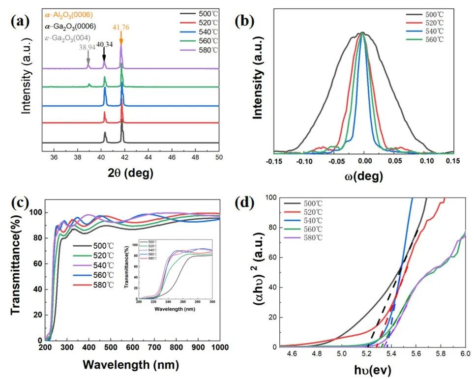
Figure 1. (a) XRD spectrum of α -Ga2O3 epitaxial film powder prepared at sapphire substrate position z=50mm, growth temperature 500-580℃, (b) (0006) crystal surface rocking curve, (c) penetration spectrum, (d) optical band gap.

Figure 2. (a) Point location of 2-inch α-Ga2O3 epitaxy (p1-p5) (b) crystal surface rocking curve of α-Ga2O3 (0006) at p1-p5 point.
Paper Information:Rapid epitaxy of 2-inch and high-quality α-Ga2O3 films by mist-CVD method
doi: 10.1088/1674-4926/44/6/062803
6、Investigation of β-Ga2O3 thick films grown via carbothermal reduction
Gallium oxide (Ga2O3) is a semiconductor material with ultra-wide band gap, which has many advantages such as ultra-wide band gap, high Baliga’s figure of merit and strong thermal stability, making it have strong application potential in the field of high power electronic devices and high temperature and deep ultraviolet detection. For example, its ultra-wide band gap makes Ga2O3 suitable for the manufacture of solar-blind UV detectors for UV-C radiation (wavelength below 280 nm). In nature, there are five different crystal phases of Ga2O3 (α, β, ε, δ, γ), in these structures, β-Ga2O3 (monoclinic crystal system) has the best thermal stability, so β-Ga2O3 is the mainstream research subject. However, due to the high requirement of single crystal β-Ga2O3 film in the epitaxial process, the preparation of large-size β-Ga2O3 single crystal is still extremely difficult.
Recently, Professor Liang Hongwei of Dalian University of Technology deposited β-Ga2O3 film by carbothermal reduction technology on c-face sapphire. According to the XRD and SEM characterization results, the research group obtained high quality β-Ga2O3 films. In this work, they systematically studied the influence of the temperature during the epitaxial process, oxygen flux, and the molar ratio of carbon powder to gallium oxide powder on the resulting film quality. The results show that there is a optimal temperature for the epitaxial process. For this growth system, this optimum temperature is 1,050℃. When the temperature is lower than this value, the gases such as Ga2O or Ga produced in the system cannot be efficiently moved to the substrate to react with the oxygen in the system to form a β-Ga2O3 film. When the temperature is too high, the kinetic energy obtained by molecules or atoms is large enough that they cannot bind well with each other, which is also unfavorable to the generation of β-Ga2O3 films. In addition, oxygen flux is also a very critical influencing factor. According to the theoretical analysis, the increase of oxygen flux facilitates the reaction of Ga2O or Ga gas to form the product —— Ga2O3. However, when the oxygen flux in the system is too much, this will destroy the parallel relationship between the oxygen atoms in the sapphire substrate and the oxygen atoms in β-Ga2O3, and thus destroy the growth process. Finally, the effect of different molar ratios between reactants on the quality of β-Ga2O3 films was explored by adjusting the amount of carbon powder. Overall, the research group considered that the most suitable epitaxial parameters are 1050℃, 20 sccm O2 and the molar ratio of carbon powder and Ga2O3. With these parameters, the reaction lasted for 2h and a β-Ga2O3 film with 25.32μm thickness was obtained.
The β-Ga2O3 film obtained by the epitaxy of carbothermal reduction technology can effectively solve the existing problems of some mainstream epitaxial methods(such as MOCVD, HVPE, and MBE), such as toxic substances involved in reaction, expensive equipment, and low speed and rate. This work can promote the research of β-Ga2O3 film by relevant institutions and lay a foundation for the development of ultra-wide band gap semiconductor materials in China.
The article is published in Journal of Semiconductors, titled “Investigation of β-Ga2O3 thick films grown on c-plane sapphire via carbothermal reduction”.

Figure 1. The SEM plane characterization results of the films obtained at different temperatures,(a) 950℃ large size, (b) 950℃ small area, (c) 1050℃, (d) 1350℃.

Figure 2. XRD of β-Ga2O3 films obtained at different molar ratios of carbon powder and Ga2O3 powder(a) 20 : 1, (b) 10 : 1, (c) 5 : 1.
Paper Information:Investigation of β-Ga2O3 thick films grown on c-plane sapphire via carbothermal reduction
doi: 10.1088/1674-4926/44/6/062804
8、Preparation of Sn doped Ga2O3 thin films and their solar blind photoelectric detection performance
The band width of gallium oxide (Ga2O3) is about 4.2-4.9 eV, and the corresponding photon wavelength of the energy is 253-295 nm, which can realize the full coverage of the solar blind range, and is a natural solar-blind detection material. At present, the cost of Ga2O3 single crystal substrate is high, the process of Ga2O3 nanomaterials preparation detector is complex, and it is difficult to produce in batch. Ga2O3 film-based solar blind detector is the most promising for commercial application. The preparation of Ga2O3 film by RF magnetron sputtering method has the advantages of fast growth rate, low process cost, good film forming quality and less environmental pollution, which is suitable for large-scale use. However, the film prepared by magnetron sputtering is amorphous or polycrystalline, the amorphous Ga2O3 film has high resistivity, and the photocurrent of the solar blind detector is small, which limits the performance parameters such as the responsiveness of the device. Sn doping is an effective way to improve the responsivity of Ga2O3 film-based solar blind detectors, but at the same time it also reduces its selectivity.
Recently, the research group of Professor Chen Haifeng from Xi'an University of Posts and Telecommunications prepared Sn-doped Ga2O3 film on the sapphire substrate by magnetron sputtering method, and studied the influence of annealing atmosphere on the solar-blind detection properties of the film. The results show that after Sn doping, the Ga2O3 solar blind detector significantly improves its response to 254 nm UV light, but also has a significant response to 365 nm UV light. Sn-doped Ga2O3-based devices annealed by nitrogen atmosphere have an optimal performance and a pronounced response to 254 nm UV light. At 20 V, photocurrent is 10μA, dark current is 5.76 pA, light-to-current ratio of 1.7 × 10⁶, response is 12.47A/W, external quantum efficiency of 6.09 × 10³%, specific detection rate of 2.61 × 10¹² Jones, response and recovery time of 378 ms and 90 ms, respectively. The consistency, stability and repeatability of the devices can meet the application requirements, and the response and selectivity need to be further improved by optimizing the film preparation and annealing process. Exploring the annealing process conditions and further improving the crystallization quality of the film has played a positive role in promoting the performance index and commercial application of the Ga2O3 solar blind detector.
This article is published in Journal of Semiconductors, titled “Preparation of Sn doped Ga2O3 thin films and their solar blind photoelectric detection performance”.

Figure 1. The XPS spectra of the Ga2O3 thin film:(a) all measured peaks, (b) Ga 3d peak, (c) Sn 3d peak, (d) O 1s peak

Figure 2. The I-t characteristic curve of the Ga2O3 solar-blind detector:(a) unannealed, (b) nitrogen atmosphere annealed, (c) air atmosphere annealed, (d) unannealed (part of (a)), (e) nitrogen atmosphere annealed (part of (b)), (f)air atmosphere annealed (part of (c)).
Paper Information:Preparation of Sn-doped Ga2O3 thin films and their solar-blind photoelectric detection performance
doi: 10.1088/1674-4926/44/6/062805
8、Preparation and photodetection performance of high crystalline quality and large size β-Ga2O3 microwires
Gallium oxide (Ga2O3) has attracted the attention and research of countries all over the world with its excellent performance, and has become a new research hotspot after gallium nitride and silicon carbide. The band width of Ga2O3 is about 4.9 eV, which has potential applications in deep ultraviolet light detection and high power electronic devices. Currently, studies based on solar-blind UV detectors of different forms of Ga2O3 are widely reported, including bulk materials, thin films, and micro-nano structures. Ga2O3 film can be grown by various methods, but the crystal quality remains to be improved.
Recently, professor Li Bingsheng of Northeast Normal University prepared large size and high crystal quality Ga2O3 micron wire via chemical vapor deposition, and studied the detection performance of micron wire-based photoconductive devices for deep ultraviolet light. The research team successfully prepared large-size Ga2O3 micron wires using carbothermal reduction oxidation(Figure 1). The micron line is up to 1 cm in length, with a smooth surface and a quadrangle cross section.Subsequently, the photoelectric detection performance of micron wire was tested, which showed obvious response characteristics to solar-blind ultraviolet light (Figure 2). Thanks to the high quality of the material, the dark current of the device is as low as 0.1 nA at 10 V bias, and the solar blind visible ratio can reach 5.8 × 10⁵, showing excellent photoelectric detection performance. The results of this study provide important references for the fabrication of high-quality Ga2O3-based micro-nano optoelectronic devices.
This article is published in Journal of Semiconductors, titled “Preparation and photodetection performance of high crystalline quality and large size β-Ga2O3 microwires”.

Figure 1. (a-b) Ga2O3 micron wire photo.(c-d) SEM images of the Ga2O3 micron line.

Figure 2. (A) I – V curves of Ga2O3 micron line under dark state and 250 nm illumination.(B) Optical response spectrum of Ga2O3 micron wire at 10 V bias.(C) Detection rate spectrum of Ga2O3 micron wire at 10 V bias.
Paper Information:Preparation and photodetection performance of high crystalline quality and large size β-Ga2O3 microwires
doi: 10.1088/1674-4926/44/6/062806
