


Member News
【Member News】Research progress in Gallium oxide materials and power devices by Mr. He Yunlong and his team from Xidian University
日期:2023-08-04阅读:1741
Progress of Gallium Oxide Materials and Power Devices
HE Yunlong, HONG Yuehua, WANG Xichen, ZHANG Zhouning, ZHANG Fang, LI Yuan, LU Xiaoli, ZHENG Xuefeng, MA Xiaohua
School of Microelectronics, Xidian University, Xi’an 710071, China
Abstract: Gallium oxide (Ga2O3) is expected to become the main force in the future semiconductor power electronics field with its advantages of large forbidden band width, high breakdown field strength and strong radiation resistance. Compared with the common wide band gap semiconductor SiC and GaN, Ga2O3 has advantages of superior Baliga’s figure of merit and lower cost in growth, and more potential for high voltage, high power, high efficiency, and small size electronic devices. The latest domestic and international research on Ga2O3 epitaxial materials, power diodes and power transistors are summarized, and the future applications and development prospects of Ga2O3 are anticipated.
Keywords: Ga2O3; epitaxial material; power diode; power transistor
1 Introduction
With the implementation of the national strategy of "carbon peak, carbon neutrality", energy conservation, emission reduction and improvement of conversion efficiency are important development directions in the energy field at present. Power semiconductor devices are the core of power conversion. In order to achieve this strategic goal, power devices with super-high power, high conversion efficiency, and small size have become a research hotspot. At present, after decades of continuous optimization of chip manufacturing, device structure, packaging and application technology, the first generation of semiconductor devices represented by Si and Ge have approached or reached the physical limit of materials, and the space for future development is limited. Therefore, relying on the existing Si-based power devices has been unable to meet the working needs of power semiconductor devices for miniaturization and high efficiency, finding and developing semiconductor materials with excellent performance has gradually become the main direction of researchers at home and abroad. The ultra-wide band gap semiconductor material represented by gallium oxide (Ga2O3) has ultra-wide band gap (about 4.8 eV) and ultra-high critical breakdown field strength (about 8 MV/cm), so it has the advantages of high breakdown voltage and high output power, and has become one of the hotspots of current research.
Compared with the common wide band gap semiconductors GaN and SiC, the mobility of Ga2O3 materials is not high, but its ultra-high breakdown field strength and fast electronic saturation speed, make it has great advantages in the field of power electronics with low on resistence under high voltage. At present, there are 6 known crystal phases of Ga2O3 materials, among which β-Ga2O3 has the highest thermal stability and the best single crystal growth quality, so it is the best choice for device preparation. As to the power electronic devices prepared based on β-Ga2O3, the Baliga’s figure of merit is 4 times that of GaN devices, 10 times that of SiC devices, and 3444 times that of Si devices. Therefore, under the same operating voltage, the β-Ga2O3 device has lower on resistance and less power consumption, which can greatly reduce the power loss of the device. In addition, the preparation process of β-Ga2O3 single crystal substrate is similar to sapphire substrate, which can be directly obtained by metal melting method. At present, the 4-inch Ga2O3 single crystal substrate process is relatively mature, and the cost is expected to be reduced to one-third of the SiC substrate of the same size, so it has great potential in aspect of low cost. Compared with GaN power devices, β-Ga2O3 power devices have higher reliability without current collapse; and they have higher breakdown field strength than GaN and theoretically have higher output power. Compared with SiC power devices, β-Ga2O3 power devices have a simple fabrication method and a planar structure can be used, which is easier to integrate. On the other hand, the thermal conductivity of β-Ga2O3 is low, which also becomes a bottleneck restricting the development of β-Ga2O3 devices. Therefore, how to improve the heat dissipation effect of the device has become a key problem to be solved urgently.
Ga2O3 is considered to be a promising material for the next generation of high power, high efficiency and low power consumption power supply system. Developed countries such as Europe countries and the United States have listed it as the next generation of strategic semiconductor materials, and carried out a series of research. This paper summarizes the latest research progress in Ga2O3 materials, power diodes and power transistors at home and abroad, hoping to provide a reference for the research of Ga2O3 material and its devices.
2 Ga2O3 Denitaxial material
The Ga2O3 material epitaxial technology mainly includes Hydride Vapour Phase Epitaxial (HVPE), Metal-Organic Chemical Vapor Deposition (MOCVD) and Molecular Beam Epitaxial (MBE), etc, among which, HVPE is the mainstream way of material growth at present, with large size, low defect density, low growth cost. However, due to a monoclinic crystal system of Ga2O3, its surface roughness is relatively higher and requires Planarization treatment. Meanwhile, it is not easy to control the epitaxial thickness due to its high growth rate. At present, the mainstream research institutions are mostly in Japan, South Korea and other countries. In 2014, Tokyo University of Agriculture and Technology in Japan adopted GaCl2 and O2 as the precursor source, and epitaxial on the (001) crystal orientation of Ga2O3 substrate by HVPE growth method, the FWHM of the rocking curve of the (002) crystal orientation is 90", and the background impurity carrier concentration is as low as 1013cm-3[1]. In 2019, Chonnam National University of South Korea introduced Pd nanoparticles and used the HVPE method to grow α phase Ga2O3 films on sapphire, with a FWHM of its rocking curve 879" and a roughness 4.98 nm[2]. In 2022, Soongsil University of South Korea grew α phase Ga2O3 film with HVPE on sapphire. The XRD rocking curve of the epitaxial material is shown in Figure 1, and the FWHM of the rocking curve of the epitaxial Ga2O3 film is 73". And a MOSFET device was made on this material, with its breakdown voltage up to 2300 V, indicating that the quality of Ga2O3 grown by HVPE was significantly improved [3].

Figure 1 The XRD rocking curve of the epitaxial material
Compared with HVPE growth method, the thickness of epitaxial material grown by MBE is accurate and controllable, but the method has low growth efficiency and cannot meet the growth requirements of large size epitaxy, which is not the mainstream method in the industry. Even so, it is still the main method of growing high-quality epitaxial materials. In 2020, the Leibniz Institute in Germany tried to improve the growth rate using metal indium assisted metal exchange catalysis through a homogeneous epitaxial Ga2O3 film layer on the (100), with a growth rate up to 1.5 nm/min and a roughness (RMS) 0.3 nm[4]. In 2020, Cornell University used the novel S-MBE method to epitaxy Ga2O3 films on sapphire and Ga2O3, respectively, and the epitaxial growth rate on sapphire was 1.6 µm/h, and the epitaxial growth rate on the Ga2O3 substrate is 1.5 µm/h. The rocking curve of the film has a FWHM of 71" and a roughness of 0.7 nm [5]. In 2022, the research team introduced In2O and SnO, which improved the growth rate of Ga2O3 film, and the FWHM of its rocking curve was 10.3" and the roughness was 0.25 nm [6], as shown in Figure 2, which is the best level of Ga2O3 growth through MBE.

Figure 2 Exaxial material test results by Cornell University
The MOCVD epitaxial growth method combines the advantages of both HVPE and MBE. It can not only obtain a large film size, but also effectively control the growth rate, which is an effective way to develop Ga2O3 epitaxial growth into industrialization. Due to the late start of this method, the quality of grown materials needs to be improved. In 2018, the University of California reported Ga2O3 films with ultra-high electron mobility using the MOCVD growth method with 176 cm2/(V·s) at room temperature, and 3481 cm2/(V·s)[7] at 54 K. In 2021, Jilin University carried out the MOCVD homoepitaxial Si-doped Ga2O3 thin film on the substrate of (100), and realized controllable doped[8] with doping concentration from 6.5×1016cm-3 to 2.6×1019 cm-3 ; In 2022, By optimizing the growth process, Ga2O3 film material was achieved, with the carrier doping concentration as low as 3.6×1016 cm-3, an electron mobility 137 cm2/ (V·s). Its FWHM of the (002) diffraction surface is 26.3", and the roughness of the film is 0.323 nm[9]. As shown in Figure 3, this is currently the best quality Ga2O3 material grown by the MOCVD method.

Figure 3 Surface roughness of MOCVD epitaxial material by Jilin University
With its excellent material performance, Ga2O3 attracts attention from researchers at home and abroad, and it is considered as the core of the next generation of power electronic devices. Therefore, power devices based on Ga2O3 materials have potential in the fields of high power, high temperature and strong radiation. Key research in Ga2O3 power devices focus on Ga2O3 power diodes and Ga2O3 power transistors.
3 Ga2O3 Power diode
At present, Ga2O3-based power diode can be divided into Schottky structure, field terminal structure, fin groove structure and PN junction structure, etc., and the parameters to evaluate the main performance of the device include breakdown voltage, on-resistance, Baliga’s figure of merit, etc.
3.1 Schottky structure
The conventional Ga2O3-based power diode is mainly composed of a Schottky contact anode and an ohmic contact cathode. In 2013, the Japanese Tamura company successfully prepared the first β-Ga2O3-based diode, as shown in Figure 4, with a breakdown voltage of 150 V[10]. In 2015, National Institute of Information and Communication Technology (NICT) of Japan used HVPE method, and achieved successfully growth of low 7 µm of epitaxial layer (doping concentration of 1×1016 cm-3), and prepared the diode based on this material. Through characteristic study of variable temperature C-V, I-V , they found that the forward turn-on current of the device conforms to the thermal electron emission mechanism, the reverse leakage current transmission conforms to the thermal field emission mechanism[11].

Figure 4 Conventional power diodes made by Tamura, Japan
3.2 Field terminal structure
It can be seen from section 3.1, there is still a big gap between the theoretical limit and the diode breakdown field strength using only conventional Schottky structure. Therefore, in order to obtain a higher breakdown voltage and Baliga’s figure of merit, the device needs to be developed and improved on the new field terminal technology. The field terminal technology mainly makes the electric field distribution of the device more uniform through the ion injection or metal electrode at the edge of the anode, so as to weaken the peak electric field at the edge of the anode electrode. In 2019, the National Institute of Information and Communication Technology in Japan injected nitrogen ions in the anode edge region of Ga2O3, and used the composite terminal structure of the field ring superimposed field plate to achieve a breakdown voltage of 1.43 kV and a on resistance [12] of 4.7 mΩ·cm2. In 2021, the University of Utah prepared the field plate structure with double-layer high-k dielectric BTO / STO, whose on resistance is as low as 0.32 mΩ·cm2, breakdown voltage is 687 V, and Baliga’s figure of merit exceeds 1 GW/cm2. The on resistance is the lowest value reported[13]. In 2022, Xidian University made the field terminal power diode by etching to form a groove structure and filling with silica dielectric. The breakdown voltage of the device is up to 6000 V, the on resistance is 3.4 mΩ·cm2, and the Baliga’s figure of merit of the device is as high as 10.6 GW/cm2[14].
Although great progress has made on the Ga2O3 field terminal structure, the lack of P-type doping of Ga2O3 material seriously restricts the development of Ga2O3 power diode towards higher performance. The researchers tried to use P-type NiOx instead of Ga2O3 to form a heterogeneous PN junction, which filled the regret of the loss of P-type Ga2O3 and has become the focus of current research. In 2020, CETC 13 took advantage of NiOx natural P type and combined it with Ga2O3 to produce a Junction Barrier Schottky diode (JBS), whose structure is shown in Figure 5. The on resistance of the device is 3.45 mΩ·cm2, the breakdown voltage is 1715 V, and the Baliga’s figure of merit exceeds 0.85 GW/cm2[15]. In 2021, Xidian University made a groove-type JBS structural power diode, the breakdown voltage of the device reaches 1340 V, and the on resistance is as low as 1.94 mΩ·cm2[16].

Figure 5 The JBS diode structure produced by CETC 13
3.3 Fin-type groove structure
In 2018, Ga2O3 diode with fin groove structure was first prepared by Cornell University in the United States. The structure is shown in Figure 6. Al2O3 dielectric was deposited above the deep groove, and the breakdown voltage of the device is up to 2440 V and the on resistance is 11.3 mΩ·cm2[17]. The advantage of the device is that the multiple fin grooves are used to separate the active region. The structure not only has a flat field terminal structure, but also adds the longitudinal field terminal, and the multiple fin grooves increase the heat dissipation area. In 2020, the research group used two-stage field plates to optimize the Ga2O3 diode with fin groove structure. The breakdown voltage of the device reaches 2890 V, the on resistance is 10.5 mΩ·cm2, and the Baliga’s figure of merit of the device is as high as 0.80 GW/cm2[18].

Figure 6 The Ga2O3 diode of the first fin-type groove structure
3.4 PN junction structure
With the fully-fledged technology of NiOx deposition, the researchers tried to combine high-quality P-type nickel oxide with N-type Ga2O3 to prepare a Ga2O3 diode with heterogenous PN junction structure, and replace the Schottky junction with PN junction to improve its pressure resistance characteristics. In 2020, Nanjing University deposited two layers of NiOx with different concentrations by changing the oxygen atmosphere and chamber pressure, and made Ga2O3 PN junction diodes on this basis. The breakdown voltage is 1860 V, the on resistance is 10.6 mΩ·cm2, and its Baliga’s figure of merit is 0.33 GW/cm2[19]. In 2021, Xidian University made a PN junction diode through magnetron sputtering. The breakdown voltage of the device is 1220 V, its on resistance is reduced to 1.08 mΩ·cm2, and its Baliga’s figure of merit reaches 1.38 GW/cm2[20]. In the same year, USTC optimized the interface between NiOx and Ga2O3 through post-annealing technology to reduce the interface state defect density, thus improving the performance of the device. After annealing, the breakdown voltage is increased from 900 V to 1630 V, the on resistance is reduced to 4.1 mΩ·cm2, and the Baliga’s figure of merit is 0.65 GW/cm2[21].
Due to the excellent characteristics of the heterogeneous PN junction formed by NiOx and Ga2O3, the diode performance of the PN junction structure has been greatly improved. Therefore, the researchers constantly combine the PN junction structure with the field terminal structure to improve the characteristics of Ga2O3 power diodes. In 2022, the NiOx of the trapezoidal countertop was made by Nanjing University and combined with Ga2O3 to prepare heterogenous PN junction diodes. The breakdown voltage reaches 2230 V and the on resistance is 1.9 mΩ·cm2[22]. In the same year, CETC the 13th Institute made the device combined the heterogeneous PN junction structure with the trapezoidal field plate, the breakdown voltage reaches 2410 V and the on resistance is as low as 1.12 mΩ·cm2, and the Baliga’s figure of merit reaches 5.18 GW/cm2[23]. In Xidian University, the heterogenous PN junction structure diode was fabricated by using the bilayer concentration of NiOx, combined with various terminal technologies such as Mg ion injection field ring and SiO2 dielectric field plate. The device structure is shown in Figure 7, NA and ND are the acceptor and the donor doping concentration respectively, and T stands for the thickness. The breakdown voltage of the device reaches 8320 V, the on resistance is 5.24 mΩ·cm2, and the Baliga’s figure of merit reaches 13.2 GW/cm2[24], which is the highest reported in the world.

Figure 7 Composite terminal structure of gallium oxide PN diode made by Xidian University
Through the above research, it can be noted that using the heterogeneous PN junction structure is still one of the most effective methods to improve the Baliga’s figure of merit. Meanwhile, in order to improve the breakdown field strength of the device and make it closer to the theoretical limit, the field terminal technology is still indispensable. Therefore, the major direction of Ga2O3-based power diodes is still aiming at increasing its breakdown voltage and reducing its on resistance. Absolutely, with the continuous improvement of the device performance, the breakdown field strength of the device is constantly approaching its theoretical limit, and the thermal stability and reliability of the device will become a more important standard for consideration.
4 Ga2O3 Power Transistor
Compared with Ga2O3 power diodes, the research on Ga2O3 power transistor is still relatively lagging behind, mainly because it is difficult to obtain the high quality epitaxial materials on the insulating substrate. At the same time, the size of high quality epitaxial materials is small, and there is less physical space for the improvement of device characteristics. Therefore, there are many problems unsolved in Ga2O3 power transistors, including low breakdown voltage, low current density, and it is difficult to prepare the enhanced mode device. The main research subjects covers the field terminal technology, vertical device technology and enhanced technology, etc. The main parameters to evaluate the device performance include breakdown voltage, on resistance, the Baliga’s figure of merit, etc.
4.1 Field Terminal Technology
Similar to the Ga2O3 power diodes, the breakdown field strength of the Ga2O3-based power transistors is far below its theoretical limit. It is imperative to develop and optimize the field terminal technology to obtain a high breakdown field strength. In 2020, CETC the 13th Institute achieved Ga2O3-based MOSFET using optimized source field plate technology, with a structure as shown in Figure 8, the power figure of merit of the device is 277 W/cm2, reaching the world's leading level[25]. In the same year, the Institute studied the influence of oxygen atmosphere annealing on the device power performance, which is also the first report in China on power performance of Ga2O3-based MOSFET. The device output power Pout is 0.4 W/mm at 1 GHz CW, the power added efficiency (PAE) is 10%, the gain is 3.2 dB[26].
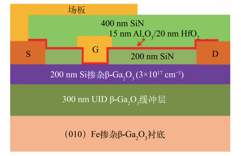
Figure 8 Ga2O3-based MOSFET made by CLP 13 Institute
In 2019, the Japanese Institute of Electronics and Communications produced MOSFET using double-layer dielectric combined with source field plate technology, and its breakdown voltage reaches 2321 V. This technology provides a stable, low-cost and effective method to promote breakdown voltage[27] for Ga2O3-based MOSFET. In 2022, the University of Buffalo used the polymer passivation layer to significantly increase the breakdown voltage of MOSFET, with the device breakdown voltage up to 8.03 kV[28]. Xidian University optimized the NiOx/Ga2O3 inerface and combined the groove technology, the on resistance of the device reached 6.24 mΩ·cm2 , the breakdown voltage was 2145 V, and the power figure of merit (PFOM) reached 0.74 GW/cm2. The value is the highest reported on lateral Ga2O3-based MOSFET at present, showing the great application prospect of Ga2O3-based MOSFET in high power, high efficiency and power electronics[29].
4.2 Vertical device technology
For lateral devices, in addition to adopting effective terminal technology to increase the breakdown voltage of the device, the gate-to-drain spacing can also be increased, which undoubtedly increases the active region area of the device. Therefore, many researchers have begun to focus on vertical devices, which can increase the breakdown voltage of devices without changing the area of their active region area, so it is one of the important directions of current research. In 2019, the National Institute of Information and Communication Technology of Japan produced vertical Ga2O3-based MOSFET through N- and Si-ion implantation doping technology, which provides an important reference[30] for the study of Ga2O3-based vertical-type devices. In 2022, the first vertical field effect transistor (VDBFET) of Mg diffusion current blocking layer (CBL) was produced by Stanford University. The switching ratio of the device reaches 109 and the breakdown voltage is 72 V. Although the breakdown voltage is very low, the report of the device provides a theoretical basis for the innovation of Ga2O3-based MOSFET in CBL structure[31].
In 2019, vertical fin Ga2O3-based MOSFET was produced at Cornell University, USA, as shown in Figure 9. The device modulates the threshold voltage of the device by controlling each fin width, and modulates the breakdown voltage through the doped concentration of the drift region. The breakdown voltage of the device is up to 2.66 kV, and the specific on-resistance is 25.2 mΩ·cm2. The device uses many key technologies, such as low-damage etching technology, fine-line lithography technology, dielectric conformal coverage technology, so it is difficult to achieve. However, it has the advantages of controllable threshold voltage, good breakdown characteristics, and good heat dissipation, etc., and provides an important support for the application of Ga2O3-based MOSFET in the field of power electronics[32].

Figure 9. Vertical fin-type Ga2O3-based MOSFET made by Cornell University, USA
4.3 Enhanced technology
The mobility of Ga2O3 material is low, usually lower than 200 cm2/(V·s). Besides, in order to obtain a higher current density, the channel layer of the material is usually thick, so the threshold voltage of Ga2O3-based MOSFET is negative (less than -20 V), which severely limits the application of the device in power conversion. Therefore, the production of high-performance enhanced power devices is the future development trend. In 2019, the U. S. Air Force Laboratory produced the enhanced Ga2O3-based MOSFET with groove gate structure with a threshold voltage of +3V at 0.1 mA/mm current density, the density of drain current greater than 20 mA/mm, current switch ratio greater than 107, and the breakdown voltage of the device higher than 198 V [33]. The gate oxygen annealing technology is adopted by CETC 13th Institute to form the gate oxide layer (OA zone), which effectively reduces the electronics in groove. The threshold voltage of the enhanced device is 4.1 V, and the breakdown voltage is above 3000 V [34]. The device structure is shown in Figure 10. In 2022, Xidian University made Ga2O3 enhanced power device by optimizing NiOx/Ga2O3 interface and combining Ga2O3 groove technology. The on resistance is 13.75 mΩ·cm2, the breakdown voltage is 1977 V, and the PFOM value is 0.28 GW/cm2. This parameter is the best indicator of Ga2O3 enhanced power device at present[29].

Figure 10 Enhanced device structure made by CETC 13th Institution
Due to the low thermal conductivity of Ga2O3 material and the defects of oxygen vacancy and gallium vacancy, the thermal performance and the carrier transport of Ga2O3 are affected. Too low thermal conductivity leads to severe self-heating phenomenon of the device, which will lead to severe decline of the device performance. Therefore, the heat dissipation efficiency becomes the bottleneck restricting the application of Ga2O3 power devices. In 2019, Xidian University adopted ion knife lift-off technology for the first time to realize the substrate transfer of Ga2O3-based MOSFET, as shown in Figure 11, the "I" in GaO@ISiC (GaO@ISi) represents the Al2O3 dielectric layer. It provides an important solution to the heat dissipation problem of Ga2O3 power devices[35]. In addition, substrate thinning is also one of the effective method to solve the heat dissipation problem of Ga2O3 power devices[36].

Figure 11 Ion knife stripping and bonding technology of Xidian University
From the above research progress, it can be seen that the optimization of field terminal technology is still one of the effective ways to raise the breakdown voltage of Ga2O3-based MOSFET. At present, the highest breakdown voltage of Ga2O3 power transistors can reach 8.03 kV. By optimizing the interface characteristics and combining the groove technology, the highest PFOM value (0.74 GW/cm2) can be obtained. Although some progress has been made in the research of Ga2O3-based MOSFET, compared with the diode, the development of MOSFET is in the initial stage, and there are still many problems to be solved.
5 Conclusion
This paper summarizes the latest research on Ga2O3 epitaxial material, power diodes and power transistors at home and abroad. Ga2O3 epitaxial materials are mainly obtained through three growth methods: HVPE, MBE and MOCVD. Among them, the growth method of MOCVD takes both the large epitaxial size and controllable growth rate into account, which is an effective way to push Ga2O3 materials to industrialization. Optimizing its growth process, preparing epitaxial materials with the large size and high quality will become the main research direction in the future. Ga2O3 power devices are mainly divided into power diodes and power transistors. At present, Ga2O3 power diode has approached the theoretical limit through the combination of heterogeneous PN junction and a variety of field terminal technologies, and is one of the closest to commercial devices. While Ga2O3 power transistor has achieved some breakthroughs with various technologies, the performance of the device still lags its theoretical limit due to the material properties and size, and the preparation technology of enhanced devices is not perfect, so technical development and theoretical research need to be continued. In addition, limited by the inherent low thermal conductivity characteristics of Ga2O3 materials, the thermal management technology of Ga2O3 power devices will also become one of the key research directions in the future.
References:
[1] MURAKAMI H,NOMURA K,GOTO K,et al. Homo-epitaxial growth of β-Ga2O3 layers by halide vapor phase epitaxy[J].Applied Physics Express,2014,8(1):015503.
[2]CHA A-N,BANG S,RHO H,et al.Effects of nanoepitaxial lateral overgrowth on growth of α-Ga2O3 by halide vapor phase epitaxy[J]. Applied Physics Letters,2019,115(9):091605.
[3]JEONGY J,PARK J-H,YEOM M J,et al.Heteroepitaxialα-Ga2O3 MOSFETs with a 2.3kV breakdown voltage grown by halide vapor-phase epitaxy[J]. Applied Physics Express,2022,15(7):074001.
[4]MAZZOLINI P,FALKENSTEIN A,GALAZKA Z,et al.Offcut-related step-flow and growth rate enhancementduring (100)beta-Ga2O3 homoepitaxy by metal-exchang catalyzed molecular beam epitaxy (MEXCAT-MBE)[J].Applied Physics Letters,2020,117(22):1-6.
[5]VOGT P,HENSLINGF V E,AZIZIE K,et al.Adsorption-controlled growth of Ga2O3 by suboxide molecular-beam epitaxy[J].APL Materials,2021,9(3):031101.
[6]VOGT P,HENSLINGFV E,AZIZIE K,et al.Extending the kinetic and thermodynamic limits of molecular-beam epitaxy utilizing suboxide sources or metal-oxide-catalyzed epitaxy[J].Physical Review Applied,2022,17(3):034021.
[7]ZHANG Y,ALEMA F,MAUZE A,et al.MOCVD grownepitaxial β-Ga2O3 thin film with an electron mobility of 176 cm2/(V·s)at room temperature[J]. APLMaterials,2018,7(2):022506.
[8]JIAO T,LI Z,CHEN W,et al.Stable electron concentrationSi-doped β-Ga2O3 films homoepitaxial growth by MOCVD [J].Coatings,2021,589(11):11050589.
[9]ZHAO C L,JIAO T,CHEN W,et al. Preparation ofhigh-thickness n--Ga2O3 film by MOCVD[J].Coatings,2022,645(12):12050645.
[10]SASAK IK,HIGASHIWAKI M,KURAMATA A,et al.Ga2O3 Schottky barrier diodes fabricated by usingsingle-crystal β-Ga2O3(010) substrates[J].IEEE Electron Device Letters,2013,34(4):493-495.
[11]HIGASHIWAKI M,KONISHI K,SASAKI K,et al.Temperature-dependent capacitance-voltage and current-voltage characteristics of Pt/Ga2O3 (001) Schottky barrier diodes fabricated on n-Ga2O3 drift layers grown by halide vapor phase epitaxy[J]. Applied Physics Letters,2016,108(13):133503.
[12]LIN C-H,YUDA Y,WONG M H,et al.Vertical Ga2O3 Schottky barrier diodes with guard ring formed bynitrogen-ion implantation[J].IEEE Electron Device Letters,2019,40(9):1487-1490.
[13]ROY S,BHATTACHARYYA A,RANGA P,et al.High-k oxide field-plated vertical (001)beta-Ga2O3 Schottky barrier diode with Baliga's figure of merit over 1 GW/cm2[J].IEEE Electron Device Letters,2021,42(8):1140-1143.
[14]DONG P,ZHANG J,YAN Q,et al.6kV/3.4mΩ·cm2 vertical beta-Ga2O3 Schottky barrier diode with BV2/Ron,sp performance exceeding 1-D unipolar limit of GaN and SiC[J].IEEE Electron Device Letters,2022,43(5):765-768.
[15]LYU Y,WANG Y,FU X,et al.Demonstration of beta-Ga2O3 junction barrier Schottky diodes with a Baliga'sfigure of merit of 0.85GW/cm2 or a 5A 700V handling capabilities[J]. IEEE Transactions on Power Electronics,2021,36(6):6179-6182.
[16]YAN Q,GONG H,ZHANG J,et al.Beta-Ga2O3 hetero-junction barrier Schottky diode with reverse leakagecurrent modulation and BV2/Ron,sp value of 0.93GW/cm2[J].Applied Physics Letters,2021,118(12):1-5.
[17]LI W,HU Z,NOMOTO K,et al. 2.44kV Ga2O3 vertical trench Schottky barrier diodes with very low reverseleakage current[C]//2018IEEE International ElectronDevices Meeting(IEDM),2018.
[18]LI W,NOMOTO K,HU Z,et al.Field-plated Ga2O3 trench Schottky barrier diodes with a BV2/Ron,sp of up to 0.95GW/cm2[J]. IEEE Electron Device Letters,2020,41(1):107.
[19]GONGHH,CHENXH,XUY,etal.A1.86-kVdoublelayeredNiO/beta-Ga2O3 verticalp-nheterojunctiondiode[J].AppliedPhysicsLetters,2020,117(2):022104.
[20]WANG C,GONG H,LEI W,et al.Demonstration of thep-NiOx/n-Ga2O3 heterojunction gate FETs and diodes with BV2/Ron,sp figures of merit of 0.39 GW/cm2 and1.38GW/cm2[J]. IEEE Electron Device Letters,2021,42(4):485-488.
[21]HAO W,HE Q,ZHOU K,et al.Low defect density and small I-V curve hysteresis in NiO/β-Ga2O3 pn diode with a high PFOM of 0.65GW/cm2[J]. Applied Physics Letters,2021,118(4):043501.
[22]ZHOU F,GONG H,XU W,et al.1.95-kV beveled-mesa NiO/beta-Ga2O3 heterojunction diode with 98.5%conversion efficiency and over million-times overvoltage ruggedness[J]. IEEE Transactions on Power Electronics,2022,37(2):1223-1227.
[23]WANG Y,GONG H,LYU Y,et al. 2.41kV verticalP-NiO/n-Ga2O3 heterojunction diodes with a record Baligasfigure-of-merit of 5.18GW·cm2[J].IEEE Transactions on Power Electronics,2022,37(4):3743-3746.
[24]JI X,LU C,YAN Z,et al.A review of gallium oxide-based power Schottky barrier diodes[J].Journal of Physics D-Applied Physics,2022,55(44):65-81.
[25]LYU Y,ZHOU X,LONG S,et al.Source-field-platedβ-Ga2O3 MOSFET with record power figure of merit of 50.4MW/cm2[J].IEEE Electron Device Letters,2019,40(1):83-86.
[26]LYU Y,LIU H,ZHOU X,et al.Lateral β-Ga2O3 MOSFETs with high power figure of merit of 277MW/cm2[J].IEEE Electron Device Letters,2020,41(4):537-540.
[27]MUN J,CHO K,DO J,et al.2.32kV breakdown voltage lateral β-Ga2O3 MOSFETs with source-connected field plate[J]. ECS Journal of Solid State Science and Technology,2019,8(7):Q3079.
[28]SHARMA S,ZENG K,SINGISETTI U,et al.Field-plated lateral Ga2O3 MOSFETs with polymer passivation and8.03kV breakdown voltage[J].IEEE Electron DeviceLetters 2020,41(6):836.
[29]WANG C,ZHOU H,ZHANG J,et al.Hysteresis-free andls-switching of D/E-modes Ga2O3 hetero-junction FETs with the BV2/Ron,sp of 0.74/0.28GW/cm2[J]. Applied Physics Letters,2022,120(11):112101.
[30]WONG M,GOTO K,HIGASHIWAKI M,et al.Current aperture vertical β-Ga2O3 MOSFETs fabricated by N- andSi-ionimplantation doping[J].IEEE Electron Device Letters,2019,40(3):431-434.
[31]ZENG K,SOMAN R,CHOWDHURY S,et al.Vertical Ga2O3 MOSFET with magnesium diffused current blocking layer[J].IEEE Electron Device Letters,2022,43(9):1527-1530.
[32]LI W,NOMOTO K,HU Z,et al.Single and multi-finnormally-off Ga2O3 vertical transistors with a breakdownvoltage over 2.6kV[C]//IEEE International Electron Devices Meeting(IEDM),2019:19-271.
[33]CHABAK K,MCCANDLESS J,MOSER N,et al.Recessed-gate enhancement-mode β-Ga2O3 MOSFETs[J].IEEE Electron Device Letters,2018,39(1):67-70.
[34]LYU Y,ZHOU X, LONG S,et al.Enhancement-mode β-Ga2O3 metal-oxide-semiconductor field-effect transistor with high breakdown voltage over 3000V realized by oxygen annealing[J].Physica Status Solidi(RRL)-Rapid Research Letters,2019,14(3):1900586.
[35]XU W,WANG Y,YOU T,et al.First demonstration of waferscale heterogeneous integration of Ga2O3 MOSFETs on SiC and Si substrates by ion-cutting process[C]//IEEEInternational Electron Devices Meeting(IEDM),2019.
[36]GONG H,ZHOU F,YU X,et al.70 μm body Ga2O3Schottky barrier diode with 1.48K/W thermal resistance,59 A surge current and 98.9% conversion efficiency[J].IEEEElectron Device Letters,2022,43(5):773-776.
