Member News
【Member News】Research progress of Professor Tang Weihua's research team in Nanjing University of Posts and Telecommunications —— Multi-pixels gallium oxide UV detector array and optoelectronic applications
日期:2023-11-10阅读:1227
Currently, significant progress has been made in the field of ultraviolet light detection based on wide-bandgap semiconductors. Photodetectors play a crucial role in the detection of ultraviolet photons, spanning various domains including image sensing, optical fiber communication, missile warning, fire monitoring, environmental surveillance, healthcare, and biological research. It is worth noting that photodetector arrays have become a pivotal component in achieving ultraviolet imaging and communication systems. These semiconductor materials are highly favored due to their unique inherent properties and resistance to external interference, leading to the widespread use of large-scale, high-performance photodetector unit arrays in areas such as image sensing, environmental monitoring, biological research, and space exploration. The advancements in these technologies are driving innovation in modern optoelectronic devices. Among them, Gallium Oxide (Ga2O3) stands out as a representative ultra wide-bandgap(UWBG) semiconductor with a direct bandgap of approximately 4.9 eV, covering the entire range of solar blind ultraviolet, making it particularly suitable for the detection of solar blind ultraviolet radiation. With the continuous advancement of deep-ultraviolet (DUV) communication and optoelectronic detection, research in this field has become a significant focal point in the scientific community. For more accurate information collection and transport, the photodetector array of many pixels is the key of the UV imaging and commnication systems, and its photoelectric performance seriously depends on semiconductor material and array layout. Therefore, this paper mainly focuses on Ga2O3 semiconductor detector array which has gained widespread attention in the field of DUV technique, from the perspective of individual device to array and its optoelectonic integration, for reviewing and discussing the research progress in design, fabrication, and application of Ga2O3 arrays in recent years. It includes the structure design and material selection of array units, units growth and array layout, response to solar blind light, the method of imaging and image recognition. Morever, the future development trend of the photodetector array has been analyzed and reflected, aiming to provide some useful suggestions for the optimizing array structure, improving patterned growth technology and material growth quality. As well as Ga2O3 optoelectronic devices and their applications are discussed in view of device physics and photophysics in detector. The first author of the paper is graduate student Lincong Shu, and the corresponding authors are Professor Weihua Tang and Associate Professor Zeng Liu. This work was supported by the Young Scientists Fund of the National Natural Science Foundation of China, the National Key R&D Program of China.

FIG. 1 Development and application of gallium oxide array detector
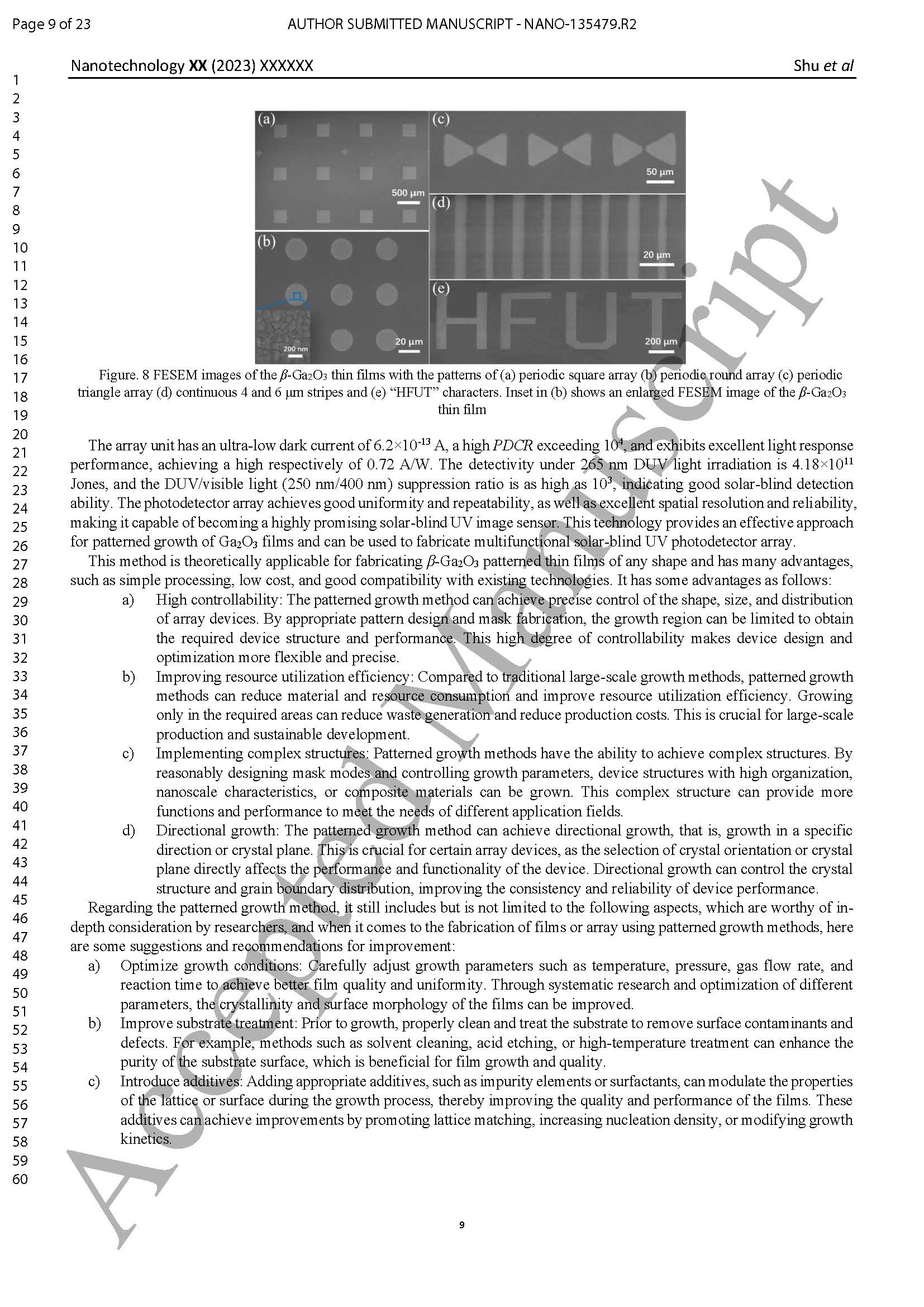
The fabrication of multi-pixels Ga2O3 UV detector array mainly includes thin film processing and patterning technology. To be more precise, thin film processing contains different types of CVD, PVD, and VPE, and patterning technology involves photolithography, etching, electrode deposition, packaged and so on. And now, photolithography technology is a commonly used microelectronic manufacturing technique for fabricating structures and devices at the micro and nanoscale. It is also feasible for fabricating array structures. Photolithography offers advantages such as high resolution, precise alignment, and high fabrication efficiency. The process involves illuminating a photosensitive resist material with a light source and using a pattern on a photomask to initiate a photochemical reaction in the resist, thereby transferring the desired pattern onto the substrate.
However, research on Ga2O3 photodetector array imaging is still not thorough enough, and the mechanism of the influence of the number and shape of array units on imaging quality is still ambiguous. In addition, many issues centered on optimizing array performance and fabrication processes remain to be solved. The main difficulties lie in the uniformity and repeatability of the photodetector array units. Patterned growth may be one of the best solutions currently available, which can improve array performance by optimizing the fabrication process. If key performance parameters such as dark current, response speed, and detectivity are further optimized, real-time dynamic imaging and precise recognition of complex images can be achieved, enriching the depth of imaging applications. Next is the selection of electrode materials and the connection and wiring layout of the photodetector unit. The selection of electrode materials significantly affects device performance, and it is also necessary to address the layout, wiring, and isolation issues between array units. The third is the expansion of photodetector array applications. Research and applications in the optoelectronic field of detection and imaging are increasingly emerging, and photodetector arrays also have great application potential in artificial intelligence neural network image recognition.
With the continuous improvement of device performance and photodetector array recognition patterns, corresponding biological feature recognition such as face recognition and fingerprint recognition may gradually be achieved, and the feasibility of array application in UV digital communication has been confirmed. Therefore, it is necessary to broaden our horizons to expand the application field of Ga2O3 photodetector arrays. Moreover, nanoscale structures have unique properties such as one-dimensional native structures, excellent light capture, surface carrier recombination, and larger surface-to-volume ratios make them very large-scale integration, one of the ideal structures for research on sensors and photodetector. Accordingly, high performance single devices from nanorod arrays have been derived. Therefore, researchers can use nanorod or microsphere devices with high performance as new array units, which may improve array performance. However, uneven and uncontrollable nanoscale structure growth remains the main cause of poor nanoscale structure performance. Therefore, patterned growth is still one of the best solutions currently available, and further research and discussion are needed on patterned growth methods.
In this article, the latest research progress on Ga2O3 photodetector arrays in recent years, covering array unit structure and material selection, unit growth and array formation methods, array unit response to solar blind UV light, optical application, and the future development trend and application in artificial intelligence and UV communication is precisely reviewed and discussed. However, facing the demanding requirements of high performance and low cost for commercial applications, most of the reported Ga2O3 photodetector arrays still have many shortcomings, such as the lack of in-depth research on array structure design, fabrication technology and effective methods for improving key performance parameters especially for the research on patterned growth methods of arrays. In addition, this paper proposes corresponding research directions or suggestions in the fabrication processes and optical applications such as imaging, UV communication and so on of photodetector arrays. As an important component of sensors, it is necessary for photodetector arrays to maintain good performance in harsh environments. However, there is currently no research on performance differences or effective ways to improve array performance in harsh environments such as high temperature and humidity, strong light, laser radiation, and electromagnetic interference. Furthermore, the application areas of array also need to be expanded urgently, which requires the attention of researchers and the continuous improvement and development of photodetector array applications.
This article is provided by Professor Tang Weihua and his team at Nanjing University of Posts and Telecommunications.
Links to related articles:
1. Solar-blind UV communication based on sensitive β-Ga2O3 photoconductive detector array,Appl. Phys. Lett., 2023, 123(4), 041103. https://doi.org/10.1063/5.0161521.
2. 16×16 Solar-Blind UV Detector Based on β-Ga2O3 Sensors, IEEE Electron Device Lett., https://ieeexplore.ieee.org/document/10115448
3. High responsivity and fast response 8×8 β-Ga2O3 solar-blind ultraviolet imaging photodetector array, Sci. China Technol. Sci., http://engine.scichina.com/doi/10.1007/s11431-022-2404-8
4. 16×4 Linear Solar-Blind UV Photoconductive Detector Array Based on β-Ga2O3 Film, IEEE Trans. Electron Devices, https://ieeexplore.ieee.org/document/9443644
5. Arrays of Solar-Blind Ultraviolet Photodetector Based on β-Ga2O3 Epitaxial Thin Films, IEEE Photonics Technol. Lett., https://ieeexplore.ieee.org/document/8337767
6. Self-Powered ε-Ga2O3 Schottky Photodiode Array Featuring High EQE Towards Solar-Blind Imaging, IEEE Photonics Technol. Lett., DOI: 10.1109/LPT.2023.3330477