


Member News
【Member News】Academician Hao Yue of Xidian University:Some New Progress of Third Generation Semiconductors
日期:2023-11-10阅读:1253

The third generation of semiconductors, with superior power characteristics, high frequency characteristics, high energy efficiency and low loss, has become the focus of the global powers game.
-- Hao Yue, academician of the Chinese Academy of Sciences and director of the Information Science Department of the National Natural Science Foundation of China
The word "dare" comes first, seeking to seal the new development of the testing industry. The 21st China Semiconductor Packaging and Testing Technology and Market Annual Conference opened in Kunshan, Jiangsu province on Oct 26. Hao Yue, academician of the Chinese Academy of Sciences and director of the Information Science Department of the National Natural Science Foundation of China, made a keynote report on the topic of " Some New Progress of Third Generation Semiconductors ". The report pointed out that the third-generation semiconductor has superior power characteristics, high frequency characteristics, high energy efficiency and low loss and other characteristics, and has become the focus of the global power game. At present, the development of the third generation semiconductor technology faces many challenges, such as high reliability, through the innovative research and development of The integration of Industry and education of semiconductor devices and materials to make it great. The formation of China's real industrial chain in the field of segmentation, so as to promote the development of science and technology and industry.
Semiconductor chips have long been at the forefront of the science and technology and industry game in major countries, and as an important branch of the field of microelectronics devices, they are of great significance to the development of the Internet of Things, information industry, weapons and equipment, biomedicine and intelligent industries. Since the beginning of this century, there have been two major achievements in the field of semiconductor science and technology and application. One is the FinFET technology below 14nm, which has promoted the continuous development of integrated circuits; The second is the third generation of Gallium Nitride, Silicon Carbide, and Gallium Oxide semiconductor device technology, which has a trend of further development and surpassing.
The third generation semiconductor refers to the semiconductor material with a bandgap width Eg>2eV, and the material with Eg>4eV is ultra-wide band gap semiconductor. The development of semiconductor devices affects national security, energy consumption and social development. In recent years, the third generation semiconductors represented by Silicon Carbide (SiC) and Gallium Nitride (GaN) and ultra-high bandwidth band gap semiconductor materials have significant advantages of high withstand voltage and low power consumption, and have become the focus of research and development and industrialization of China's power semiconductor industry.
The advantage characteristics of the third generation semiconductor
In terms of industry and technology expectations, the third generation semiconductor has high power characteristics, high efficiency and low loss characteristics, and high frequency characteristics.
First, superior high power characteristics

The third generation (wide band gap) semiconductor has obvious advantages in high temperature and high voltage, high power, high current density and low on-resistance. In the past, due to the small drive power required, fast switching speed, silicon-based MOSFETs occupy the mainstream in applications below 600V, due to low on-loss, fast switching speed, high withstand voltage grade, high working junction temperature, convenient drive, silicon-based IGBTs occupy the 600V~6500V high voltage application market. Compared with silicon-based IGBT, Silicon Carbide wide band gap semiconductors have more potential performance breakthroughs.
Silicon Carbide suitable for medium and high voltage, in terms of above 650V voltage level. The main application scenarios are new energy vehicles, photovoltaic inverters and some application fields of industry. Gallium Nitride suitable for low and medium voltage, below 650 volts, the main application scenarios are fast charge, mobile phone fast charge consumer electronics fast charge. With the popularity of new energy vehicles and electric vehicles, the automotive industry has also joined today's chip competition. Unlike the traditional automobile manufacturing industry, the development of electric vehicles largely relies on the development of semiconductor devices. As a result, the market share of third-generation semiconductors is also gradually increasing.
Second, superior high efficiency and low loss characteristics
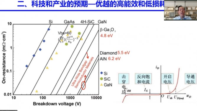
The on-resistance is nearly 1/1000 of the silicon device (at the same voltage/current level), which can greatly reduce the on-loss of the device. wide band gap semiconductors provide low impedance to reduce on-off losses and improve energy efficiency.
Third, superior high frequency characteristics
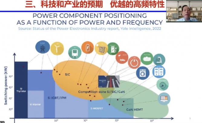
GaN electronic devices are epitaxial growth barrier layer/channel layer material on the substrate material. This structure enables 2DEG with high density and high mobility (speed), which is key to realizing microwave and high-power semiconductor devices.
High frequency and high voltage is the largest characteristic of the third generation of semiconductor material devices, the first used third generation of semiconductor material devices including Silicon Carbide (SiC), high frequency and short wave devices, the current application market has been mature, while Silicon Carbide (SiC) devices are also suitable for extreme working environments. The application of 42GHz Silicon Carbide CMESFET in the field of military radar and communications has become a field of competition among countries.
Fourth, new Gallium Oxide semiconductor devices (ultra-wide bandgap semiconductors)

Wide band gap semiconductor materials have been able to support the development of high performance semiconductor devices. In recent years, the academic community is developing ultra-wide band gap semiconductor Gallium Oxide, Ga2O3 has a band gap of 4.8 eV. Ultra-wide bandgap semiconductor has higher breakdown voltage and higher power density in theory, which provides a new idea for the development of high power and high voltage devices.
Compared with the current industry hot third generation semiconductor GaN and SiC, Ga2O3 power devices have lower on-resistance under the same withstand voltage condition, applied in the field of electrical energy conversion will achieve lower power consumption and higher conversion efficiency. Therefore, in recent years, Gallium Oxide semiconductors have become the international research hotspot of semiconductors and the commanding heights of technological competition among major countries.
Since 2018, under the leadership of Academician Hao Yue, XIdian University has achieved high-speed performance improvement of Gallium Oxide power diodes and power transistors through a series of technological innovations such as independent Gallium Oxide MOCVD equipment, high-quality Gallium Oxide epitaxial materials, and new structures and processes of high-voltage devices, and achieved a number of milestones. The research level of Gallium Oxide power devices in China has entered the forefront of the world.


Ultra wide band gap semiconductor becomes the focus of the game
In recent years, carbon-based electronic materials and devices have become a research hotspot in the international semiconductor field. Among them, the ultra-wide band gap semiconductors represented by diamond have broad application prospects in detectors, electronic devices and optical switches.
On August 12, the U.S. Department of Commerce issued provisional final regulations on ECAD software required for integrated circuits with GAAFET (Gate-all-around Field Effect Transistor) structures; Diamond and Gallium Oxide as the representative of the ultra-wide band gap semiconductor materials; And new export controls on four technologies, including pressure gain combustion (PGC), used in gas turbine engines. Ultra-wide band gap semiconductor becomes the focus of the game.
The challenges facing the development of the third generation semiconductor
The 5G era is speeding up, with semiconductor devices widely used in aerospace, radar detection, communications and other industries, and new energy electric vehicles and big data centers becoming more popular. The development of wide band gap semiconductors has brought more possibilities for the future development of semiconductor devices, but there are still many problems to be solved.
The challenges in the field of Gallium Nitride are: whether the frequency can be higher; Problems with high linearity and low operating voltages; Whether Gallium Nitride materials can be further improved on 6-inch, 8-inch silicon substrates or even 12-inch; Whether high-voltage (10,000 volts) power electronics can be made even higher; And high-reliability device issues.
In the field of Silicon Carbide, the first challenge is to achieve the perfect substrate material with large size and low defects; In terms of ultra-high pressure, super power and low loss devices, whether it can be done higher; The problem of high reliability devices.
In addition, wide band gap, other compounds and Silicon heteroisomeric integrated circuits, can achieve Gallium Nitride and Silicon-base CMOS at the same time. In terms of wide band gap semiconductor device and circuit design methodology, Silicon and Gallium Arsenide are different, so how to realize the advantages and avoid the disadvantages in design and packaging and combinational optimization is also quite concerned in the industry.
