


News Trends
【World Express】Outstanding Performance in Gallium Oxide Etching
日期:2023-12-08阅读:1459

Ga2O3 has the best etching effect when using MOCVD reaction cavity to guide gallium-containing organic molecules onto the epitaxial layer.
With the rapid development, Ga2O3 has begun to influence the power device market. Due to the opportunity to manufacture a high-quality bulk substrate from the melt, this class of ultra-wide bandgap semiconductors can achieve superior device performance at a very competitive cost.
Over the past decade, the performance of this class of power devices has developed by leaps and bounds. Key breakthroughs include the manufacture of devices with a breakdown voltage of more than 8 kV and a breakdown field strength of more than 5 MV/cm, whose performance exceeds the theoretical limits of SiC and GaN. However, the performance of Ga2O3-based devices has not yet reached a level close to the theoretical limit, in part due to the lack of suitable, highly controllable, damage-free etching processes.
Controlled etching and material removal are fundamental steps in the manufacture of many different types of semiconductor devices. The ability to remove material is just as important as the ability to deposit it - the pair of complementary processes are able to shape the semiconductor material into a tightly defined device architecture.
Prior to etching, the active region of many devices is often protected by dielectrics, such as SiOx or SiNx. The same is true for Ga2O3 based devices. However, it is not easy to find a non-destructive etching process that avoids affecting the performance of the device or does not affect the reliability of the device.
Many β-Ga2O3 based devices are manufactured using a variety of etching processes. The processes include dry etching, wet etching, photochemical etching and metal-assisted chemical etching. Unfortunately, all of these forms of etching exhibit limitations, such as producing surface damage, sloping sidewalls, and anisotropic etching along certain crystal planes. Therefore, none of these methods are suitable for the production of high-performance devices.
A more promising technique is the use of steam based in situ etching in the reaction chamber of the growth tool, such as the use of MBE and MOCVD technologies. By its very nature, this epitaxial growth method enables etching and regrowing epitaxial layers and dielectrics without destroying the vacuum, resulting in a cleaner interface. Because MOCVD grows the highest quality β-Ga2O3 epitaxial layer, this reactor is the best choice for integrating the growth and etching processes together.
Agnitron is a leading supplier of β-Ga2O3 Epitaxial layer growing MOCVD reactors with a reputation, and its equipment is now installed in many world-class laboratories. What may be less well known, however, is that Agnitron reaction chambers can be used for in situ etching of Ga2O3 films, substrates and related alloys. This article will next explore the etching of β-Ga2O3 using a metal-organic source containing gallium and chlorine.

With customer feedback in mind, Agnitron made a major upgrade to its current UV exposure unit. The device now includes a directional focusing light tube that precisely focuses UV power onto a specific wafer as the film grows. This enhanced setup allows the film to grow next to an unirradiated wafer under UV light during the same run.
Etched with MBE
Growing Ga2O3 with MOCVD involves a reaction of gallium and oxygen precursors, and the deposition rate is usually determined by the concentration of gallium introduced into the reaction cavity. However, when reactive oxygen species are lacking in the reactor, the gallium precursor will have a different effect on the surface of the etched substrate or epitaxial film.
For MBE, this etching process is well known. As Ga2O3 grows, the formation of Ga2O3 and its volatile low oxide Ga2O competes with it - the growth rate of Ga2O3 is reduced when a higher gallium flux falls on the substrate in an oxygen-deficient environment (what actually happens is that the material is etched from the Ga2O3 surface, not grown on it).
When these occur, coupled with hypoxia, highly volatile low-oxide Ga2O is formed, and Ga2O desorbs from the surface rather than promoting Ga2O3 growth. Therefore, it is impractical to accelerate the growth rate of Ga2O3 using standard MBE growth processes. Given this phenomenon, many researchers have turned to etching Ga2O3's surface with gallium metal in the MBE reaction chamber. This is reported to be a low-damage etching technique in which gallium reacts with Ga2O3.
Etching with MOCVD
ASU's Nidhin Kalarickal team has relevant experience in gallium etching of Ga2O3 using MBE reaction chamber, and we worked with them to study etching Ga2O3 using MOCVD technology. Together, we demonstrated that in the absence of oxygen, gallium-containing metal-organic precursors, such as triethylgallium (TEGa), can perform in-situ etching of Ga2O3 in the MOCVD reaction chamber. Again, the etching results from the reaction of gallium with Ga2O3, which produces the volatile low-oxide Ga2O, but the process begins with the homogeneous decomposition of TEGa. When TEGa is exposed to temperatures of about 350 ° C or higher (from the substrate temperature), pyrolysis occurs, creating moving gallium adsorbed atoms on the surface. The stable organic ethylene byproducts produced during pyrolysis are expelled from the reactor via exhaust gas with minimal interaction with the substrate surface.
To monitor the in situ etching rate, we took advantage of the significant refractive index difference between the β-Ga2O3 film and the underlying sapphire substrate. The etching rate was measured by installing a fiber optic reflectometer operating at 470 nm in the Agilis 100.
With customer feedback in mind, Agnitron made a major upgrade to the current UV exposure unit. The device now includes a directional focusing light tube that precisely focuses UV power onto a specific wafer as the film grows. This enhanced setup allows the film to grow next to an unirradiated wafer under UV light during the same run.
With this setup, we investigated the effect of various process conditions on the etching rate of (201) oriented β-Ga2O3 epitaxial films grown on C-plane sapphires. In particular, we also investigated the TEGa molar flow rate, substrate temperature, and chamber pressure. These experiments showed that we could increase the etching rate from about 0.3μm/hr to 9μm/hr (see Figure 2).

Figure 1. Agnitron MOCVD reactor with blue LED glowing in the center of a 2-inch wafer (left). (Right) The red trace is the measured reflectance data, and the blue trace corresponds to the reflectance data for the estimated etching rate. The estimated etching rate is 9μm/hr.
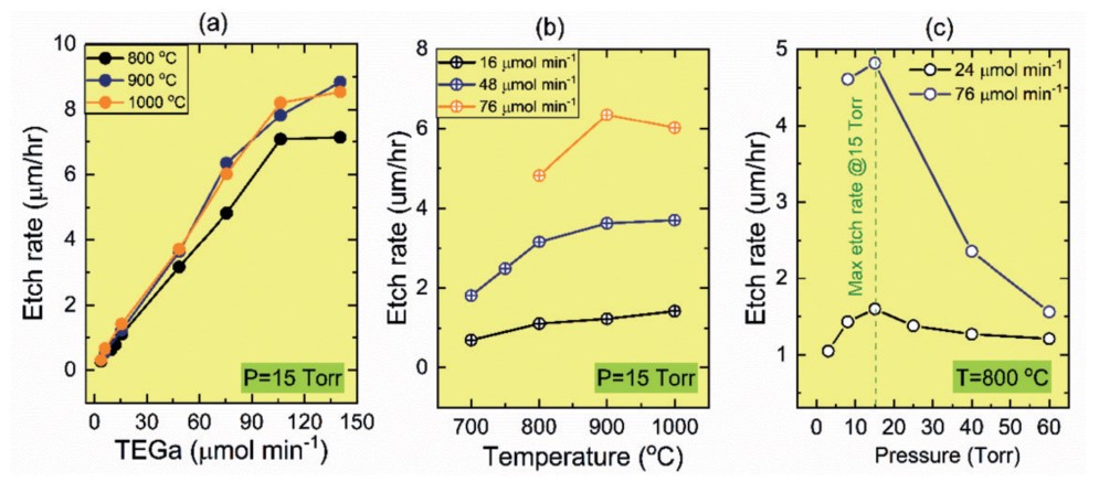
Figure 2. Etching rate of β-Ga2O3 on sapphire in relation to etching parameters. (a) Etching rate in relation to the molar flow rate of TEGa at a constant pressure of 15 Torr and substrate temperatures of 800°C, 900°C and 1000°C. (b) Relationship of etching rate to substrate temperature at constant pressure of 15 Torr and TEGa molar flow rates of 16μmol/min, 48μmol/min and 76 μmol/min. (c) The relationship between etching rate and chamber pressure at substrate temperature of 800°C and TEGa molar flow rates of 24 and 76μmol/min.
We found that for low TEGa molar flow rates (i.e., less than 100μmol/min), the etching rate increases linearly as the flow rate increases (see Figure 2(a)). However, at higher flow rates, the etching rate increases only slightly before saturation. When the etching conditions are in a linear state, the low oxide reaction rate is high enough to consume all of the gallium adsorbed atoms provided by reaching the substrate surface. Thus, the etching rate is limited by the molar flow rate of TEGa provided, resulting in the observed linear relationship. Conversely, as the number of gallium adsorbed atoms supplied increases beyond the point at which the low oxide reaction can consume them, the etching rate will increase sublinearly, after which saturation is reached.
Another influencing factor for increasing the etching rate is the substrate temperature. Higher temperatures will speed up the etching rate, but only to a certain extent, with saturation occurring above 900 ° C. When saturation occurs, the etching rate at saturation depends on the TEGa molar flow rate (see Figure 2(b)). When the substrate temperature is below 800 ° C, the etching rate is limited by the low oxide reaction rate rather than by the TEGa flow rate provided. In this case, an increase in substrate temperature will result in a higher etching rate, and excess gallium will be present on the substrate surface. This is the other way around at higher temperatures, resulting in the consumption of all supplied gallium in a low oxidation reaction. The etching rate is then limited by the TEGa flow rate provided, resulting in saturation of the etching rate. The pressure in the MOCVD reaction chamber also affects the etching rate (see Figure 2(c)). The maximum etching rate occurs at 15Torr.

Figure 3. (AlxGa1-x)2O3 etching rate on sapphire as a function of aluminum composition. The etching was performed at 3 Torr pressure, 800°C substrate temperature, and 24μmol/min TEGa molar flow rate.
In addition, we use TEGa etching (AlxGa1-x)2O3. In this particular study, we compared the etching rates of Ga2O3, (Al0.11Ga0.89)2O3 and (Al0.22Ga0.78)2O3 films, which were all grown on a C-plane sapphire substrate by MOCVD. Using a reactor pressure of 3.0 Torr, a substrate temperature of 800 ° C, and a TEGa molar flow rate of 24 μmol/min, we determined that the etching rates of Ga2O3 were about 1.0 μm/hr, while the etching rates of (Al0.11Ga0.89)2O3 and (Al0.22Ga0.78)2O3 were only 0.2 μm/hr and 0.17 μm/hr, respectively. These findings suggest that AlGaO is an etching terminator and that (Al0.11Ga0.89)2O3 is just as good as (Al0.22Ga0.78)2O3 in this respect.
Control metal droplets
One limitation of gallium in situ etching is the creation of gallium metal residue, which is deposited on the etched surface. Residues present during etching in MBE and MOCVD reaction chambers must be removed before proceeding to the device process step.
One successful way to remove gallium residue is to etch the sample surface with hydrochloric acid. But since this can only be done outside the growing room, the etched surface is exposed to air and prone to contamination, which can harm device performance. Therefore, it is impractical to etch with hydrochloric acid, which in turn is the only option after etching in the MBE reaction chamber.
With MOCVD, gallium droplets can also be removed in situ using halogen-based metal-organic precursors. There is an option that we have validated that involves the use of tert-butyl chloride (TBCl). This organic compound is also known for in-situ and selective regional etchings of GaN. When gallium droplets form on the etched Ga2O3, they are converted to volatile derivatives of GaClx and released, leaving a clean surface. Cleaning can be performed at small flows of TBCl, while etching can also be performed at higher flows.
Interfacial Silicon
One problem plaguing Ga2O3's growth is the accumulation of silicon at the interface between the film and the substrate. Silicon is produced regardless of the process conditions, dopants in the substrate, and whether it is grown by MBE or MOCVD technology.
The interfacial silicon is thought to come from the silicon-based polishing process of the substrate, and may also come from the cyclic siloxanes that the Ga2O3 substrate is exposed to air. But regardless of its source, its presence can harm device performance. For example, in FETs, parasitic conductive channels are created at the film/substrate interface to prevent the device from pinching.
The concentration of interfacial silicon can be reduced by etching the Ga2O3 substrate in concentrated hydrofluoric acid for about 30 minutes before loading into the growth chamber. This method does not eliminate the interfacial silicon, but rather reduces its concentration, causing it to be partially compensated by the acceptor impurity (magnesium or iron), which diffuses from the semi-insulated substrate into the interface during epitaxial film growth. Recently, in collaboration with Krishnamoorthy's group at UC Santa Barbara, we used this technology to produce and publish a high performance, kilovolt class Ga2O3 MESFET with a record power value of over 350 MW cm-2.
We also investigated whether gallium etching can remove interfacial silicon. We etched the Ga2O3 substrate to a depth of about 300nm using TEGa, then exposed the surface to TBCl to remove the gallium metal deposits, after which an unintentionally doped β-Ga2O3 layer of about 650nm thickness was grown. After performing all of these steps in the same reactor without destroying the vacuum, we carefully examined the sample with secondary ion mass spectrometry (SIMS), quantifying the unintentionally doped epitaxial layer and the concentrations of silicon, carbon, hydrogen and chlorine at the interface between this film and the substrate (see Figure 5 (b)). SIMS 'results showed that the unintentionally doped epitaxial layer was clean, with concentrations of each impurity below the instrument's detection limits. No binding of carbon and chlorine was observed at the interface, but the concentration of hydrogen increased slightly, while the concentration of silicon was unaffected. We attribute the persistence of the latter to strong covalent bonds containing silicon and oxygen atoms.

Figure 4. Image taken from the outside through a transparent quartz tube reactor during Ga2O3/ sapphire etching. The dark coating on the wafer surface (left) is due to gallium metal deposits, and on the right is the wafer surface after the gallium metal deposits have been removed.
We can conclude that gallium etching is suitable for processing sizes of various device architectures as well as regrowing ohmic contact and dielectric materials such as SiO2 and Al2O3. However, the promise of this technique for removing interfacial silicon is beyond doubt.

Figure 5. Etched and reepitaxy sample (a), and secondary ion mass spectrometry (SIMS) depth profile of silicon, carbon, hydrogen, and chlorine impurities. (b)
Evaluating Surface Roughness
Most importantly, when any substance etches the film or substrate, it leaves a smooth surface. To see if this is the case with TEGa, we used this precursor to blanket etch Fe-doped (010) and Sn-doped (001) β-Ga2O3 substrates to a depth of 350nm.
According to AFM maps, the roughness after etching is low, and the smoothness increases with the substrate temperature (see Figure 6). The root-mean-square surface roughness after etching has a value of about 3nm. In addition, parallel elongated grooves were found in the microscopic images of this form, which were also observed on the surface of the epitaxically grown β-Ga2O3 film.
We also used a scanning electron microscope to examine the material after etching. In addition to evaluating the morphology of the fully etched film using this technique, we also studied the structures formed by the etched patterned SiO2 hard mask (see Figures 6 (e) and 6 (f)).
Optimizing process conditions, such as TEGa flow rate, substrate temperature, pressure, and overall reactor air flow, can further improve surface quality. In addition, we found that exposing TEGa etched surfaces to TBCl for longer periods of time resulted in reduced surface roughness. We found this when performing etching experiments using a pair of approximately 5 mm by 5 mm (010) Fe-doped β-Ga2O3 wafers3 cut from the same substrate. For the sample etched in TEGa alone, the surface roughness was about 21nm, while the sample etched in TEGa exposed to TBCl for about 20 minutes had a surface roughness of about 8nm (see Figures 6 (g) and 6 (h)). We attribute the smoother surface to TBCl's effective removal of gallium droplets and its ability to gently etch Ga2O3 surfaces.
Other Etchings
In addition to TEGa, we have investigated etching Ga2O3 with other organic molecules. In addition, trimethyl gallium (TMGa) was studied with the expectation that it would etch Ga2O3 in the same way as TEGa. However, our initial etching experiments using TMGa did not produce any signs of Ga2O3 etching. Conversely, exposing the Ga2O3 surface to TMGa for a long period of time also resulted in the formation of a black coating on the surface. We believe that the deposited coating is caused by carbon in methyl groups, a byproduct of TMGa's pyrolysis process that prevents gallium from entering the surface. The true intrinsic mechanism of coating formation is unknown.
We have shown that TBCl can remove gallium metal deposits from etched surfaces of TEGa, and can also etch Ga2O3. For a molar flow rate of only 50 μmol/min (the lower value used to remove gallium metal deposits), the etching rate is too small to measure. However, when this rate is increased by at least a factor of 10, etching of Ga2O3 by TBCl can be observed, provided that etching is performed at high substrate temperatures (over 800 ° C).

Figure 6. (a) etched (010) β-Ga2O3 surface Atomic Force Microscope (AFM) image, (b) etched (001) β-Ga2O3 surface23 AFM, (c) etched (010) β-Ga2O3 surface2 Scanning3 Electron Microscope (SEM) image, (d) SEM image of etched (001) β-Ga2O3 surface, (e) SEM image showing pattern etched Ga2O3 (010) sample using SiO22 hard mask, (f) SEM image showing pattern etched Ga2O3 (001) sample using SiO hard mask (g). No exposure in TBCl, TEGa etched (010) β- Ga2O3 substrate 2D AF2M3 image (g) and exposed under TBCl for 20 minutes, TEGa etched (010) β- Ga2O3 substrate 2D AF2M3 image (h). All AFM images were taken from a scan area of 5 μm × 5 μm.
Agnitron's Evaluation
Shubhra Pasayat, University of Wisconsin-Madison
"Agnitron's one-of-a-kind experience and advanced equipment technology make it one of the leading manufacturers of MOCVD systems with products covering a wide range of material systems, including dual-use systems. Their excellent expertise in various material systems and the fact that custom reactor designs can meet specific user needs and requirements piqued my interest, hence I chose the Agnitron MOCVD reactor for my own laboratory.
I recently purchased a dual-purpose GaN/Ga2O3 Agilis 100 reactor from Agnitron that is initially configured for high temperature nitride growth and can also be easily converted to Ga2O3 growth. Very much looking forward to the installation and start-up of the unit. Throughout the process so far, I have been very impressed with the excellent customer support provided by Agnitron. Their team was responsive, engaged in informative discussions and resolved any issues or queries in a timely manner. This great experience further solidified my confidence in Agnitron as a reliable, customer-oriented company.
In the future, I plan to expand my laboratory with the addition of another Agnitron MOCVD reactor, possibly the Agilis Mini. Based on my interactions and experiences so far, I particularly recommend Agnitron as the ideal partner for any MOCVD needs. Agnitron's commitment to customer satisfaction, combined with their expertise and cutting edge technology, is a well-deserved industry choice. I am confident that their continued support will make a significant contribution to the success of my research efforts."
Hongping Zhao, Ohio State University
"It is a pleasure to express my satisfaction with the two Agnitron MOCVD devices I purchased for my research at Ohio State University. The first device was the first two-chamber GaN device delivered in 2017, and the second was the Ga2O3 device delivered in 2018. The two-compartment Agilis reactor is a GaN device that has been used to develop II-IV-N2 based GaNs and novel nitride semiconductors. The performance and functionality of the device met my expectations. Two-compartment GaN devices have been used to demonstrate high-quality GaN epitaxy and the successful development of ZnGeN2, ZnSnN2 and their heterostructures and III-N alloys. Agnitron is constantly innovating and we are currently considering upgrading the device to further enhance its usefulness.
The Ga2O3 MOCVD system is very efficient. Agnitron's Agilis 100 is an industry standard and many thanks to Agnitron for their support of the MOCVD system and the help provided by their strong technical team. This equipment allows us to do our job well and produce world-class Ga2O3 materials.
Agnitron's customer support for OSU has been excellent. The team is responsive, engaged and addresses queries or issues that arise in a timely manner. They are reliable partners who are ready to provide guidance when needed. Based on my experience, I am happy to choose Agnitron and would be happy to recommend it to other researchers."

Figure 7. Spectral reflectance monitoring of Ga2O3/ sapphire etch using TBCl at 25 Torr reactor pressure and 900°C substrate temperature. In a single etching experiment, the TBCl flow rates varied from 315μmol/min to 505μmol/min, 1026μmol/min and 1450μmol/min, corresponding to labeled layers Etch# 1, Etch#2, ETCH #3 and Etch# 4, respectively. The etch rate varied between 0.55μm/hr and 2.23μm/hr.
We used a fiber optic reflectometer to monitor the spectral reflectance of the Ga2O3 process grown on TBCl etched sapphires (see Figure 7). In this study, we used a reaction chamber pressure of 25 Torr and a substrate temperature of 90 ° C in the Agilis 100 reactor. The TBCl molar flow rates were 315 μmol/min, 505 μmol/min, 1026 μmol/min and 1450 μmol/min. As the flow rate increased, the period of spectral reflection oscillations decreased, indicating an increase in etching rate. For a maximum flow rate of 1450 μmol/min, the etching rate exceeds 2 μm/hr. This is significantly lower than TEGa's fastest etching rate. TEGa is a more effective etching agent that can use a smaller molar flow rate.
We did a lot of experiments similar to TEGa. The etching rates of Ga2O3 films exposed to TBCl were investigated at different reactor pressures, different molar flows of TBCl, and a range of substrate temperatures and oxygen flows. Repeating observations based on TEGa etching, we found that there is an optimal reaction chamber pressure for rapid etching, in this case 25 Torr (see Figure 8(a)). For constant pressure and temperature, the etching rate increases linearly with increasing TBCl flow (see Figure 8 (b)).
At higher temperatures, the etching rate of TBCl to Ga2O3 increases. For lower substrate temperatures, a fairly high TBCl flow rate is required to obtain a measurable etching rate. For example, at a substrate temperature of 700 ° C, we must use a TBCl molar flow rate of more than 1000 μmol/min to observe etching, and even then we can only achieve a rate of 0.15μm/hr (see Figure 8 (b)). But when we raise the temperature to 900 ° C, the same flow rate will increase the etching rate to 1.65μm/hr. Although improved, it is still much slower than the etching rate of TEGa, again highlighting the inefficiency of TBCl, especially at low substrate temperatures. We also explored the effect of introducing oxygen during TBCl etching Ga2O3 (see Figure 8(c)). However, it was not successfully demonstrated that the reduced etching rate could be due to the redeposition of Ga2O3 in an oxygen environment.
We also applied TBCl to the etching of (Al0.13Ga0.87)2O3 grown on a sapphire substrate. Similar to TEGa etching, the presence of aluminum in the Ga2O3 matrix reduces the etching rate, again suggesting that AlGaO can be used as an etching terminator for TBCl.
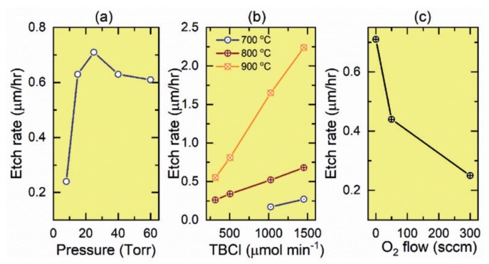
Figure 8. The etching rate of β- Ga2O3 on sapphire as a function of the etching parameters when TBCl etching agent is used. (a) Relationship between etching rate and chamber pressure at substrate temperature of 800°C and TBCl molar flow rate of 1450 μmol/min. (b) Relationship between etching rate and TBCl molar flow rate at constant pressure of 25 Torr and substrate temperature of 700°C, 800°C, 900°C. (c) Relationship between etching rate and oxygen flow rate at 25 Torr constant pressure and 1026 μmol/min TBCl molar flow rate.
Power Product Series
To achieve the etching results just discussed, our staff at Agnitron drew on 15 years of innovation experience in the field of compound semiconductors. While many of the studies detailed in this article involve the Agilis 100, these studies can also be performed on other platforms within our MOCVD product family.
The Agilis 100 is our most popular MOCVD/CVD system, known for its small footprint and versatility. In addition to the β-Ga2O, the system is also a very good choice for a variety of other experiments.
The Agilis 100 integrates ultraviolet and blue range optical reflectometers into the Imperium analytical control software, which provides real-time measurements of growth rate and thickness. Another feature is that UV exposure can be selected during growth, effectively controlling Ga2O3 film purity by reducing residual carbon and managing defect at the point. In addition, the Agilis100, as well as all of our other MOCVD/CVD systems - enables seamless switching between air source and gas distribution (sprinkler) configuration within two hours after maintenance. Another feature is the ability to add precursor dispensing nozzles for process improvements or wafer carrier cleaning, increasing the appeal of our devices for a variety of applications.
In order to address the high cost and gas consumption of wafers in research and development, it is necessary to grow on a single large area wafer. Our β- Ga2O3 MOC3VD/CVD reactors, particularly the Agilis 500/700, can now accommodate wafers up to 4 "and 6" in diameter, respectively. These larger multi-wafer reactors have the same footprint as the Agilis 100 and can help researchers looking to grow larger diameter wafers through matching production lines.
At the heart of most of our tools are proprietary vertical growth chambers with high-speed rotating disk reactors capable of operating at more than 1,300 revolutions per minute. Using materials science and design engineering, we minimize the chance of any deposits inside the chamber reaching the wafer surface.
The unique flow dynamics in our high-speed rotating disk reactors inhibit particle recirculation, thus keeping the area above the wafer clean and free of deposits. Another advantage of the high speed rotation of the rotary disk reaction chamber is that it allows for a higher degree of control, ensuring even thickness distribution.
Recently, we delivered the Agilis Mini to a number of universities. Earlier this year, we installed a facility at the University of Notre Dame in Indiana that will use high-purity materials to study quantum computing. We also shipped an Agilis Mini to ASU for the high temperature growth of AlGaN/BN compounds. The appeal of this particular model is that it has the same performance and versatility as the Agilis 100, but with a smaller footprint and an affordable price.
Our product line-up is constantly expanding. Soon we will launch the Agnitron GOX 300, a fully automated production Ga2O3 MOCVD/CVD system that offers more features for larger wafers. In addition, Agnitron is proud to commit to continuous improvement and customer support to ensure that each new generation of Agnitron reactors provides a more reliable and versatile experience for process engineers. We are committed to working with researchers and industry partners around the world to continually push the boundaries of semiconductor technology. Another major advance planned for launch in the third quarter of 2023 is the first MOCVD/CVD reactor designed specifically for research and development purposes, featuring high-temperature, low-pressure metal-organic precursor delivery. This ground-breaking innovation further expands the capabilities of MOCVD/CVD technology. Initially, the feature will be available on the Agnitron Agilis 100 reactor, making it the first reaction chamber capable of delivering precursors into the reactor at temperatures up to 200 ° C. The breakthrough enables researchers to explore the growth of new compounds and heterostructures through MOCVD/CVD, facilitate the development of novel and improved devices, as well as study new elements as potential dopants.
In addition, we are honored to patent this class of technology, which upgrades the nozzle gas distribution design. This system, combined with the rapid rotation of our rotating disk reactor, enables excellent thickness and doping uniformity of the epitaxial layer.
The success we have achieved over the years has helped us play a key role in important projects. These include the results of the AFRL SBIR project, which aims to develop Ga2O3 growth on a large area substrate. In this project, we plan to use the Agnitron Agilis 700 and GOX 300 systems to scale up the growth of Ga2O3 epitaxial structures, from small substrates to substrates 4 inches in diameter and above.
In short, Agnitron's hardware Engineering department is constantly improving equipment to ensure that each new generation of Agnitron reactors provides process engineers with increased reliability and versatility. In addition, we continue to support research activities, such as the etching work described in this article. By supporting and advancing all aspects of Ga2O3, we are helping developers of these ultra-bandgap oxides race along the path from device development to commercialization, ushering in a new era of high-voltage power electronics.
