


Expert Interview
【Expert Interview】Professor Zhang Hui, founder of Hangzhou GAREN SEMI: "100 Gallium Bloom Together" - Casting method breaks through technical barriers and lays the foundation for large-scale industrialization!
日期:2024-06-28阅读:3004
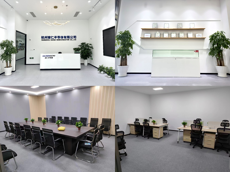
Company Profile
Hangzhou GAREN SEMI Co., Ltd. was established in September 2022, is a technology enterprise focusing on the research and development, production and sales of Gallium Oxide and other Gallium Oxide semiconductor materials. Relying on the National Key Laboratory of Silicon and Advanced Semiconductor Materials of Zhejiang University and Hangzhou International Science and Technology Innovation Center of Zhejiang University, the company has formed a research and development, production and operation team with academicians of Chinese Academy of Sciences as the chief consultant and rich industry experience.
GAREN SEMI leads the industry innovation, successfully pioneered the casting process and other Gallium Oxide single crystal growth technology, and achieved a 6-inch substrate and 2-inch (010) substrate production technology breakthroughs. The company has mastered the core technologies of the whole chain of Gallium Oxide growth, processing and epitaxy, and obtained more than 10 international and domestic invention patents, helping the domestic Gallium Oxide related industries to get rid of international monopoly and blockade. To provide customers with fully independent intellectual property rights of high-quality Gallium Oxide substrate products.
The company's products include Gallium Oxide polished wafers of different sizes, crystal orientation and resistivity, and customizable Gallium Oxide seed crystals and ingots. The products are mainly used in power electronic devices for national grid, new energy vehicles, rail transit, 5G communication and other fields.

Guest Introduction
Zhang Hui is a professor at the School of Materials Science and Engineering and Hangzhou International Science and Innovation Center, Zhejiang University. He is mainly engaged in applied research on low-dimensional materials and new energy before 2019. At present, he is mainly engaged in the research of Gallium Oxide single crystal growth, wafer processing and defect control. A new kind of melt method Gallium Oxide single crystal growth technology with independent intellectual property rights, casting method, has been developed, and overcome many bottlenecks of czochralase growth technology. He has published more than 190 academic papers in Nat. Comm., Adv. Mater. and other international famous journals, and has been authorized more than 20 invention patents. In 2008, he won the first prize of Science and Technology of Zhejiang Province (ranked third), and in 2013, he won the second prize of National Natural Science (ranked second). In 2015, he was selected into the national 10,000 "Young Top Talents" program, and supported by the National Natural Science Foundation of China Outstanding Youth Fund. In September 2022, Hangzhou GAREN SEMI Co., Ltd. was established as the founder to launch the industrialization of Gallium Oxide single crystal materials.

AGOA:Introduction of your company team
Our team was established in 2018. Under the design and guidance of Academician Yang Deren, the academic leader, our team members took the lead in the research and development of Gallium Oxide single crystal materials in the National Key Laboratory of Silicon and Advanced Semiconductors of Zhejiang University. By 2020, the team carried out a pilot trial of Gallium Oxide single crystal at Hangzhou International Science and Technology Innovation Center of Zhejiang University. In recent years, our team has been growing, and the core members have joined Hangzhou GAREN SEMI Co., LTD., and has grown into an excellent R & D and production team with academicians of Chinese Academy of Sciences as the chief consultant. The R&D staff has many years of research and development experience in the growth, processing and testing of single crystal of Gallium Oxide. The background covers the fields of physics, chemistry, materials and semiconductors, forming a multi-disciplinary cross integration, and has rich experience in company operation and capitalization.
AGOA:The technical advantages and highlights of your company's external publicity
Casting method is a new melt method for the growth of Gallium Oxide single crystal created by our team, which is also one of the technical advantages of our company. We have successfully fabricated 6-inch Gallium Oxide single crystal by casting and processed them into 6-inch double-sided polishing wafer doped with UID (unintentionally doped), semi-insulated and conductive types, which makes us a member of the Gallium Oxide 6-inch Club. Casting method has many significant advantages in industrialization: first, the casting method has low cost, compared with other methods, the amount of precious metal Ir in the casting method is greatly reduced, after our preliminary calculation, reduced by more than 80%; At the same time, because the iridium crucible is exposed to less area in the oxidizing environment, the loss of each crucible is also small, which makes the cost of the casting method significantly reduced, with the potential to promote large-scale industrialization. The domestic iridium reserves are relatively limited and the price is high, which is a limit that can not be ignored for industrialization, so reducing the amount and loss of iridium is the only way to industrialization. Second, the casting method is simple and controllable, its process flow is short, high efficiency, size is easy to enlarge, and automatic crystal growth can be realized in the future. Third, the casting method has complete independent intellectual property rights, and the patents of China, the United States and Japan have been authorized, laying a solid foundation for breaking through the monopoly of foreign technology and realizing the substitution of domestic production. We believe that casting method has outstanding advantages and is expected to become a new generation of Gallium Oxide single crystal production technology.
In addition, we have also made great breakthroughs in the Czochralase method. By developing atmosphere control technology and temperature gradient control technology, our team has solved the long-standing problems of floating matter, interface stability and twin problems, overcome the technical bottleneck of the growth of Gallium Oxide single crystal by Czochralase method, and has launched unique products.
AGOA:Introduction of your company's Gallium Oxide products
Our company has a complete range of products, including different sizes, crystal orientation and resistivity of Gallium Oxide polished wafer, customized Gallium Oxide seed, crystal ingot and so on. Starting from Q2 this year, we have also been developing epitaxial wafer of Gallium Oxide, and are expected to launch commercially available products in Q4. The company's products are mainly used in power electronic devices for the national grid, new energy vehicles, rail transit, 5G communication and other fields.
In addition to the 6-inch Gallium Oxide single crystal substrate, we recently introduced a new product, the 2-inch wafer-grade (010) Gallium Oxide semi-insulated substrate. As far as I know, there are very few units and companies in the world that can provide this kind of crystal substrate, and most of the sizes you can buy before are 10mm× 15mm. On the one hand, the crystal size of the crystal face can not be so large, on the other hand, the processing of large size (010) substrate is also a huge challenge. Aimed primarily at scientific users, the (010) substrate has excellent physical properties and epitaxy among the mainstream crystal faces commonly found on Gallium Oxide substrates. First, the (010) substrate has the highest thermal conductivity; Second, (010) substrate has faster epitaxy growth rate, and the epitaxy difficulty is much lower; Third, power devices prepared based on (010) substrate usually have superior performance. We believe that the launch of this product will further demonstrate the excellent properties of Gallium Oxide materials.

AGOA:Your company's positioning and development plan in the direction of Gallium Oxide industrialization
We specialize in the development and production of Gallium Oxide substrates and epitaxial wafer. Compared with Silicon Carbide and Gallium Nitride which have formed a certain industrial scale, Gallium Oxide is still in the early stage of industrialization at this stage. "Expensive" and "poor quality" are still the obstacles on the road of Gallium Oxide industrialization. The pursuit of cheap and high-quality Gallium Oxide single crystal materials is always the goal of GAREN SEMI. The company will adhere to the long crystal route of the casting method and greatly reduce the use of the precious metal iridium. Through continuous iterations, the price of Gallium Oxide is reduced to below that of Silicon Carbide. In addition, the company will also develop other non-guide molding routes, including iridium free technology, through the integration with the casting process, to further reduce the cost of Gallium Oxide. With upstream and downstream to carry out industrial cooperation, through the device to find the problem in the material, strive to improve the quality of materials, for the domestic device manufacturers to provide material product protection.
According to the company's strategic planning, the company has achieved the goal of Gallium Oxide 2 inches, 4 inches, 6 inches, and will further break through 8 inches in the future. However, at present, we believe that it is more important to improve product quality and reduce cost, and crystal size is no longer the bottleneck of Gallium Oxide applications.
AGOA:What is your estimate of the output value, size and future market share of your existing or upcoming production lines?
The current R&D and production site of the company has reached 1,100 square meters, and we will expand it to more than 3,500 square meters in the next year. At present, we have built a 2-inch casting process mass production line, and have completed the pilot test of 2-inch Gallium Oxide substrate, the yield has exceeded the Silicon Carbide; At the same time, we have also achieved small batch production of 4 inch and 6 inch substrates. The company's products can meet the current demand. Gallium Oxide is a relatively new wide band gap semiconductor, although it has not been fully recognized by the market, but the market prospect is very good, the future will be able to occupy an important share in the semiconductor material market. We believe that as long as the heart to seriously grow a good crystal, do a good job of industrialization, the future market will have a place for us.
AGOA:For the industrialization of Gallium Oxide, what do you think is the development prospect from the perspective of enterprise? What are the possible turning points in the future?
We all know that Gallium Oxide has large band gap, high breakdown field strength, and large BFOM, so it is generally believed in the industry that Gallium Oxide has great advantages in the preparation of power devices. For the Gallium Oxide industry, new energy vehicles, high-voltage power transmission and transformation, photovoltaic inverters, etc., are all application fields with good prospects for development. Of course, Gallium Oxide also has great advantages in the preparation of radio frequency devices and detectors, and these related fields are also suitable for the application of Gallium Oxide materials. At present, the price of Gallium Oxide substrate is expensive, which is one of the important factors limiting industrialization, in the future, if the cost of Gallium Oxide single crystal substrate can be reduced to the cost of the same size of silicon carbide under the premise of ensuring high crystal quality, then the Gallium Oxide market may have further development. Of course, P-type doping and heat dissipation of Gallium Oxide are problems that need to be overcome, which requires the collaboration of academia and industry to jointly promote.
AGOA:From the perspective of your company, which talents of Gallium Oxide do you prefer?
I often told team members that the research and development of Gallium Oxide materials must not stay in the laboratory, and must go out to achieve industrialization. GAREN SEMI's mission is to achieve the industrialization of Gallium Oxide single crystal materials. At present, the technical route of producing large-size Gallium Oxide crystals by casting method has been completed, and the next step is mainly process optimization and subsequent iterations. Therefore, the company is in urgent need of talents who understand the principle of crystal growth, master the design of thermal field and understand the transformation of equipment. Since the hardness of Gallium Oxide is not high, the processing of Gallium Oxide seems simple, but the problems of Gallium Oxide, crushing, damaged layer and other problems caused by cleavage are the key to the quality of products, and there is a shortage of excellent Gallium Oxide processing talents in the market. Epitaxy is the key to connect the substrate and the device. This year, GAREN SEMI focuses on promoting the epitaxy of MOCVD and HVPE, and very welcome excellent talents to join.
AGOA:Has your company had any good news about Gallium Oxide business or technology recently?
As mentioned above, recently, the company successfully prepared high-quality 6-inch Gallium Oxide (β-Ga2O3) single crystal substrate by casting method, becoming a domestic industrialized company that has mastered the preparation technology of 6-inch Gallium Oxide single crystal substrate. At the same time, a new product, 2-inch wafer-grade (010) Gallium Oxide semi-insulated single crystal substrate, was also introduced. We will soon be introducing larger (010) Gallium Oxide substrates.
AGOA:For the service content of alliance before, do you think there are any shortcomings that can be improved?
The alliance has done a lot of excellent work in information sharing, personnel exchange and other aspects. In the future, we hope that more enterprises can become the member unit, and jointly provide advice and suggestions for the alliance to promote the development of Gallium Oxide industry.
AGOA:What kind of services do you expect alliance to provide?
The alliance is expected to provide assistance in industrial collaboration, information sharing, academic exchanges, news dissemination, industry prospect planning and analysis, and promote exchanges and cooperation between enterprises, universities and research institutes and governments to achieve win-win results.
