


Member News
【Member News】GAREN SEMI Wafer Grade (010) Gallium Oxide Single Crystal Substrate Diameter Breakthrough of 3 inch
日期:2024-08-01阅读:1109
In July 2024, Hangzhou GAREN SEMI Co., Ltd. made a breakthrough in Gallium Oxide crystal growth and substrate processing technology, and successfully prepared a 3-inch wafer-grade (010) Gallium Oxide single-crystal substrate, which is the largest size reported in the world at present, reaching the international leading level.
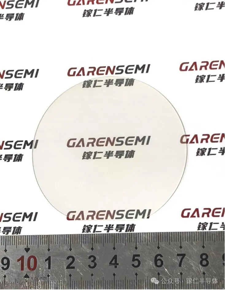
3 inch wafer-grade (010) Gallium Oxide single crystal substrate
Among the main crystal faces of Gallium Oxide single crystal substrates, (010) substrate has excellent performance in terms of physical properties and epitaxy. Firstly, the (010) substrate has the highest thermal conductivity, which is conducive to improving the performance of power devices; Second, (010) substrate has a fast epitaxial growth rate; Third, the device prepared based on (010) substrate has better performance. At present, GAREN SEMI launches wafer-grade (010) Gallium Oxide single crystal substrate products, which are targeted at the scientific research market to meet the demand for (010) substrates in the field of scientific research and promote industry-university-research collaboration in the industry. Hangzhou GAREN SEMI Co., Ltd. is mainly engaged in the research and development and production of Gallium Oxide and other semiconductor single crystal materials. It has been approved as a national technology-based medium and small enterprise, and an innovative medium and small enterprise in Zhejiang province, and has led the approval of a number of projects such as "Lingyan" by Zhejiang Science and Technology Department, with strong production and research and development strength. Previously, GAREN SEMI, together with the Advanced Semiconductor Research Institute of Hangzhou International Science and Technology Innovation Center of Zhejiang University and the National Key Laboratory of Silicon and Advanced Semiconductor Materials, successfully prepared high-quality 6-inch unintentionally doped and conductive Gallium Oxide (β-Ga2O3) single-crystal substrate using the casting method independently created by Academician Yang Deren's team. In April 2024, Hangzhou GAREN SEMI Co., Ltd. launched a new product 2-inch wafer-grade (010) Gallium Oxide semi-insulated single crystal substrate, and achieved independent mass production of 2-inch (010) Gallium Oxide Gallium Oxide substrate, breaking the international monopoly. In the future, the company's R & D team will continue to carry out independent innovation work, and gradually break through lower cost and higher quality Gallium Oxide substrates, promote the high-quality development of the Gallium Oxide industry, and help the development goal of "carbon neutrality" and "carbon peak".
Company Profile
Hangzhou GAREN SEMI Co., Ltd. was established in September 2022, is a technology enterprise focusing on the research and development, production and sales of Gallium Oxide and other semiconductor materials. The company has created a new technology for Gallium Oxide single crystal growth, and has more than ten international and domestic invention patents, breaking through the monopoly and blockade of Western countries such as the United States and Japan on Gallium Oxide substrate materials. Based on solving the major national needs, GAREN SEMI will be deeply engaged in the continuous innovation of the Gallium Oxide upstream industry chain, and strive to provide product guarantee for the development of China's power electronics and other industries.
For more information about GAREN SEMI and its products
Please visit our official website: http://garen.cc/
Or contact us:
Mr. Jiang :15918719807
Email: jiangjiwei@garen.cc
Mr. Xia :19011278792
Email:xianing@garen.cc
