


Paper Sharing
【Member Papers】University of Electronic Science and Technology of China Professor Luo Xiaorong's team β-Ga₂O₃ Latest Progress
日期:2024-08-09阅读:959
Recently, the joint research team of Professor Luo Xiaorong from UESTC and Special Researcher Xu Guangwei from USTC has made the latest progress in the degradation model and reliability reinforcement technology of NiO/β-Ga2O3 heterojunction transistors. The study was titled as “Experimental investigation on the instability for NiO/β-Ga2O3 heterojunction-gate FETs under negative bias stress", was published in the Journal of Semiconductors. Dr. Zhuolin Jiang, UESTC, is the first author, Professor Xiaorong Luo of UESTC and Researcher Guangwei Xu of UESTC are co-corresponding authors.

Research Content and Graphics
NiO proved to be very suitable for β-Ga2O3 power devices, but the mutated NiO/β-Ga2O3 heterojunction may produce serious trap effects, including degradation of threshold voltage (VTH) and current under negative bias stress, which seriously affect the operation and use of the device. The instability mechanism of NiO/β-Ga2O3 heterojunction gate field-effect transistor (HJ-FET) under different gate stresses and stress times has been investigated experimentally by UESTC and USTC, which provides important theoretical guidance for studying the reliability of NiO/β-Ga2O3 heterojunction devices in power electronics applications.
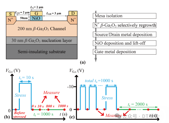
FIG. 1 (a) Schematic diagram of NiO/β-Ga2O3 HJ-FET cross-section and its manufacturing process; (b) monopulse; (c) delayed multi-pulse experimental process
In this paper, NiO/β-Ga2O3 heterojunction gate FET is manufactured according to the experimental steps shown in FIG. 1(a), and then the pre and post stress test shown in FIG. 1(b) and the delayed multi-pulse stress test shown in FIG. 1(c) are carried out respectively.
As shown in Figure 2(a), when VG,Str=-5V, the VGS-IDS curve hardly changes in the voltage region from -7.5V to -5V, while in the region from -10V to -7.5V, the IDS current is reduced by the impulse, but the VGS-IDS curve gradually returns to the initial value when tr=1000s. A similar phenomenon can be observed in the VGS-IGS curve, as shown in FIG. 2(b). The ΔVTH extracted from FIG. 2(c) shows an increase after NBS and a gradual decrease with the increase of tr. After stress withdrawal tr=1000s, VTH almost returns to the initial value. Figure 2(d) shows that IGS,off decreases by 84% at VG,Str=-5V and then gradually returns to its initial value. In addition, VG,Str=-10V causes IGS,off to drop by about 87%. It can be seen from Figure 3(a) that the degradation mechanism of the device changes under high VG,Str stress. When VG,Str=-20V, the subthreshold and linear region currents of the transfer characteristics increase after NBS, while the current in the off state region (-10V<VGS<-9V) hardly changes. A high VG,Str stress results in a decrease in ∆VTH and a near-permanent negative degradation, compared to an increase in ∆VG,Str caused by NBS, while a higher VG,Str results in a greater permanent negative drift, as shown in Figure 3(b).
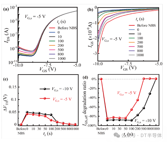
FIG. 2 Monopulse experiment. (a) VGS-IDS; (b) VGS-IGS changes; (c) ΔVTH; (d) IGS,off degradation
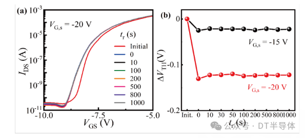
FIG. 3 Monopulse experiment. (a) The change of VGS-IDS at VG,Str=-20V; And (b) ΔVTH extracted under VG,Str=-15V/-20V stress
In this study, NBS experiments for a long times were also performed on another NiO/β-Ga2O3 HJ-FET with the same structure, which was not treated with any electrical stress. The curves at tr=2000s almost coincided with those immediately after completing NBS ts=1000s, indicating that no recovery process had occurred, as shown in Figure 4(a). The extracted ∆VTH indicates that when ts<20s, the device characteristics are relatively stable and do not start to drift. However, when ts≥20s, VTH starts to move negatively and finally shifts negatively by about 2V, while no recovery sign appears when tr=2000s, as shown in FIG. 4(b).
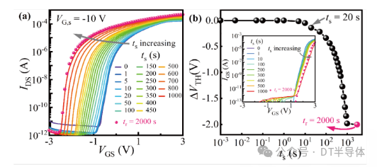
FIG. 4 NBS experiment with ts increase. (a) VGS-IDS change; And (b) extracted ΔVTH
In this paper, an interfacial dipole ionization model is proposed to explain the mechanism of HJ-FET's almost permanent decline under NBS conditions. As shown in Figure 5(a), the presence of interfacial dipoles cancels out the internal electric field generated by ionized impurities in the space charge region (SCR) due to the discontinuity of the interfacial energy band of the NiO/β-Ga2O3 heterojunction. The larger VG,s creates an extremely large electric field at the interface, causing some of the interfacial dipoles to ionize into electrons and holes, as shown in Figure 5(b). Under the stress electric field, the electrons and holes move in the direction of β-Ga2O3 and NiO, respectively, and compound with the ionizing charge in the SCR, causing the SCR to thin, the on-resistance to decrease, and the VTH to shift negatively and not recover, as shown in Figure 5(c).
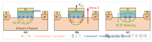
FIG. 5 Schematic diagram of degradation mechanism of NiO/β-Ga2O3HJ-FET. (a) Initial state; (b) at NBS; And (c) after NBS
The effect of stress on the electrical characteristics of NiO/β-Ga2O3 HJ-FET under different stress voltages and stress times is studied. At lower VG,s and ts values, the NiO trap traps electrons, which reduces gate injection of electrons, resulting in lower leakage current. Fortunately, it fully recovers after a longer tr. As the stress voltage or stress time increases, ionization of the interfacial dipole widens the current conduction path, resulting in an increase in current and a negative VTH shift. This is a near permanent degradation for the NiO/β-Ga2O3 heterojunction and should be taken into account in engineering.
