


Expert Interview
【Expert Interview】Prof Feng Qian:Focus on lmproving Material Uniformity to Support the Practical Application of Gallium Oxide
日期:2024-08-16阅读:2488
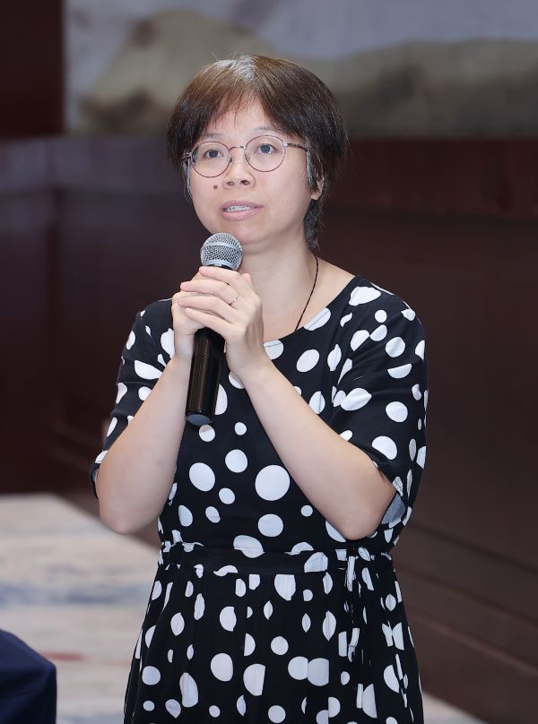
Expert Profile
Now she is a professor and doctoral supervisor of School of Microelectronics, Xidian University. She has been engaged in the research of wide band gap/ultra-wide band gap semiconductor materials and devices for a long time. At present, her main research work focuses on theoretical simulation of ultra-wide band gap semiconductor Gallium Oxide materials, epitaxial growth, and the study of solar-blind UV detectors, high-voltage switching Schottky Diodes and MOSFET devices. She has published more than 50 papers in international well-known journals and conferences such as IEEE Electron. Device Letter, IEEE Trans. Electron Devices, Applied Physics Letters, and applied for/authorized more than 40 patents. She has won three provincial and ministerial awards and one second prize of National Technological Invention Award. She has undertaken and participated in a number of national ministerial-level projects such as National Natural Science Foundation Projects, Key Projects of Natural Science Foundation, National Major Science and Technology Projects, and National Key Research and Development Programs.
AGOA:The teacher's team briefly introduced the current research direction, research progress, research results, etc
Our team is currently focused on the epitaxial growth of Gallium Oxide thin film materials and the preparation of electronic devices. As for the growth of Gallium Oxide thin films, pulsed MOCVD growth technology is mainly used to improve the migration of gallium atoms on the substrate surface, prolong the migration time, improve the film quality and reduce the surface roughness. The use of pulse In as a surfactant improves the growth rate of the film, reduces the oxygen vacancy content, improves the crystal quality of the material, and reduces the surface roughness of the film to less than 1nm, while the use of Si source pulse growth technology realizes the electron concentration of 3Í1019cm-3, and the mobility can still reach 50cm2/Vs excellent performance. In the research of Gallium Oxide Schottky Diode, our work is still focused on improving the breakdown voltage of the device and reducing the on-resistance technology. In addition, P-type ZnNiO with wider bandgap is used to study the structure of JBS, JTE and other devices, and the specific contact resistance of the device is 3.2 mΩ·cm2, the breakdown voltage is 2910V, and the PFOM is 2.65GW/cm2.
AGOA:What was the opportunity for you to start researching Gallium Oxide?
At first, I noticed Gallium Oxide because at the IEDM meeting in December 2013, NICT Japan published an article on Gallium Oxide MOSFET devices, which showed the excellent current switching ratio and high temperature characteristics of MOSFET devices. At this time, Gallium Nitride devices are becoming more and more mature and gradually moving towards application and marketization. Academician Hao Yue believes that we need to seek semiconductor materials with better performance to meet future needs, so he suggested that I pay attention to the research progress of this material and related devices, and carry out the initial material preparation research based on PLD devices. Since then, I began to research Gallium Oxide materials and devices.
AGOA:The team researched the difficulties encountered at present or those recently cracked
At present, the research difficulties we have encountered mainly focus on the preparation of high-performance Gallium Oxide materials. Throughout the development of electronic devices, it is not difficult to find that in the development process of Si, SiC or GaN power devices, the improvement and innovation of its structure is not particularly much, through the comprehensive use of a variety of terminal structures to improve the breakdown characteristics of the device, the use of Superjunction structure to reduce the on-resistance of the device. However, there are proprietary material growth equipment and technology for each material, which is not universal. That is to say, for the characteristics of each material, it is necessary to develop material growth equipment and technology that match. At present, the performance of Gallium Oxide devices is mainly limited by the material quality. Although Agnitron of the United States designed MOCVD equipment for the growth of Gallium Oxide material, the structure of the equipment is still in further optimization and improvement, and the structure of the reaction chamber of the equipment is still adjusted through the test results of the material, that is to say, the quality of the material is still in the process of gradual improvement, and there is still a large gap from its theoretical characteristics. Therefore, we are also exploring the growth methods of Gallium Oxide materials, including how to inhibit the compensation effect of the background carriers of undoped films and how to improve the mobility of the carriers.
AGOA:What aspects of the research of Gallium Oxide materials will you pay more attention to? Why?
Regarding the research of Gallium Oxide materials, I may pay more attention to the homogeneity and consistency of material properties at present. After all, to promote the practicality of Gallium Oxide, mainly focused on the preparation of high-performance devices and modules, the same requires the consistency and stability of device performance, and these in addition to the device preparation process related, more important to determine the homogeneity and consistency of material properties.
AGOA:Do you have any suggestions for the current research difficulties of Gallium Oxide?
Now raising the quality of Gallium Oxide thin film, personally, I think may be through the development of MOCVD equipment to replace currently used HVPE technology high speed growth, this will greatly improve the quality of Gallium Oxide thin film, at the same time by multiple chip growth at the same time reduce the cost of MOCVD technology, may be the ultimate way of material with high quality Gallium Oxide thin film. On the other hand is the acquisition of P-type materials, we can try to achieve oxide P-type films (such as Li doped NiO) and stable hole concentration by doping, rather than based on vacancy or defect, because this will cause instability of hole concentration and electrical performance, which will pose a great threat to the long-term application and reliability of the device.
AGOA:In your opinion, what kind of cooperation between schools and enterprises is more conducive to the production of Gallium Oxide?
Schools may be better at the analysis and research of internal mechanisms, while enterprises are better at understanding the needs of the market, but the satisfaction of market needs still revolves around the solution of existing problems. Both enterprises and schools can focus on the solution of a certain problem, but the emphasis is different. Enterprises mainly focus on the adjustment of technical solutions, while schools focus on the in-depth analysis of the changes brought about by technical solutions, and can provide guiding directions or conclusions on the basis of analysis, so as to reduce the experimental cost and time cost of enterprises and promote the research of Gallium Oxide.
AGOA:What experiences can you share with young scholars and researchers engaged in Gallium Oxide research, as well as those who will be engaged in Gallium Oxide research in the future?
At present, a large number of researches on Gallium Oxide have been carried out. Therefore, young scholars who want to engage in the research of Gallium Oxide need to focus on urgent technologies or key problems, and try to conduct experiments from multiple perspectives in order to achieve breakthrough progress. However, in the process, they will certainly face numerous problems to be solved and failures again and again. It is hoped that all of you have a strong anti-frustration ability to continue to carry out the research, and in the process of continuous discussion, thinking, adjusting the direction, and finally obtain good results.
AGOA: What are your suggestions for alliance services?
The alliance can provide a good platform for researchers and enterprises to carry out multi-faceted cooperation to promote the rapid development of Gallium Oxide.
I suggest that the alliance can link the material research structure and the device research structure more closely and do a good job in the middle. Real-time follow-up of the material research structure of the wafer and device structure performance feedback, according to the information feedback to reflect the main defect affecting the performance and life of electronic devices, which also promote the improvement of material quality.
