


Member News
【Member News】Fujia Gallium Industry Gallium Oxide Epitaxial Wafer Online——Open the Second Growth Curve
日期:2024-08-30阅读:1157
Have a goal in mind and a direction under your feet. Hangzhou Fujia Gallium Industry Technology Co., LTD. (hereinafter referred to as Fujia Gallium Industry) has always adhered to the industrialization orientation, actively assisted the industrial ecological construction in the field of Gallium Oxide and contributed to the realization of the full link of domestic Gallium Oxide "single crystal - epitaxy-device". Since the establishment of the company, Fujia Gallium Industry has focused on the research and development and industrialization of Gallium Oxide single crystal substrate and has achieved a breakthrough in the growth technology of Gallium Oxide (EFG) 6-inch Gallium Oxide single crystal, and can achieve a stable supply of 4-inch Gallium Oxide wafers.
The industrial development of new materials is linked, and only by first making beads into chains can we achieve clusters of chains and clusters into potential. In the early stage, Fujia Gallium industry targeted at the Gallium Oxide single crystal substrate material end, and was committed to providing universities and research and development institutions with cost-effective Gallium Oxide wafers. In order to accelerate the development of Gallium Oxide industry, build a bridge between the supply and demand of Gallium Oxide materials and devices, and realize the coordinated development of upstream and downstream, the company will launch a variety of Gallium Oxide epitaxial wafer, to provide better services for colleagues in the field of Gallium Oxide.
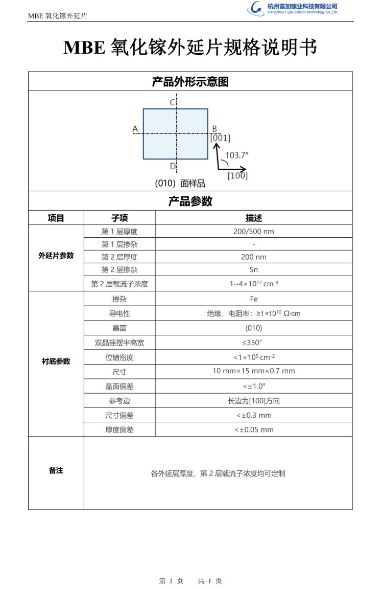
This paper introduces the Gallium Oxide epitaxial film product prepared based on molecular beam epitaxy technology (FIG. 1), referred to as MBE Gallium Oxide epitaxial wafer, which is mainly used in lateral power devices. This product adopts a double-layer epitaxial structure of unintentional doping layer and Sn doping layer, and the substrate material is semi-insulated (010) Fe doped Gallium Oxide. Among them, the carrier concentration of the doped layer of conventional products is 1-4e17 cm-3, the mobility is > 80 cm2/V·s, and the surface roughness is < 2 nm (Figure 2). For other detailed indicators, please refer to the relevant technical specifications (Annex 1).
The electrical performance of this MBE Gallium Oxide epitaxial wafer has entered the current international advanced ranks (Figure 3). We are conducting epitaxial wafer device verification in a number of well-known institutions, continuous improvement and optimization, rapid response to application needs, and accelerate the process of Gallium Oxide full-link localization.
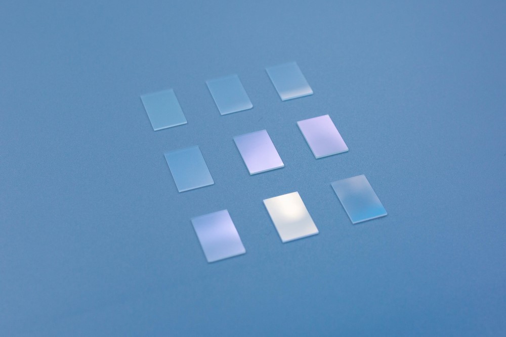
Figure 1: MBE Gallium Oxide Epitaxial Wafer

Figure 2: AFM of MBE Gallium Oxide Epitaxial Wafer
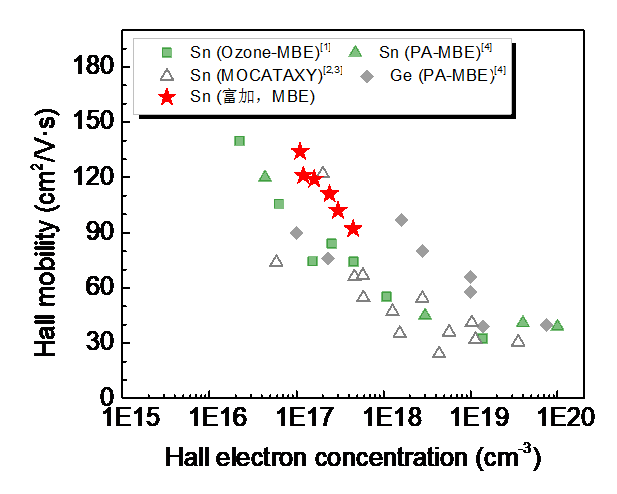
Figure 3: Summary of electrical properties of Gallium Oxide films prepared by domestic and international based on MBE
[1]Applied Physics Express, 2012, 5(3): 035502.
[2]Applied Physics Letters, 2020, 117(22): 222102.
[3] APL Materials, 2020, 8(2): 021104.
[4]Applied Physics Express, 2017, 10(4): 041102.
Annex 1:
About Fujia Gallium
Hangzhou Fujia Gallium Technology Co., LTD., founded on December 31, 2019, is the first "hard technology" enterprise registered by Hangzhou Institute of Optics and Fine Mechanics. With the vision of "Making the World Use Good Materials", the company focuses on the industrialization work of wide bandgap semiconductor Gallium Oxide materials. Mainly engaged in the growth of Gallium Oxide single crystal materials, Gallium Oxide substrate and epitaxial wafer research and development, production and sales, the products are mainly used in power devices, microwave radio frequency and photoelectric detection fields.
At present, the company has won a number of honors: In 2022, it won the Zhejiang Province Science and Technology Small and Medium-Sized Enterprise; National High-Tech Enterprise in 2023; In 2024, it will be awarded as Hangzhou Enterprise High-Tech Research and Development Center and Zhejiang Special Small and Medium-Sized Enterprise. It undertook one Gallium Oxide project for the National Development and Reform Commission and participated in three national and provincial projects from the Ministry of Science and Technology, Zhejiang Province, and Shanghai. In addition, it has obtained 12 international patents authorized (6 in the United States and 6 in Japan), 40 domestic patents authorized, 3 trademark certification and registration of "Fujia Gallium Industry", and 3 software copyrights (crystal growth control software).
For more information about Hangzhou Fujia and its products
Please visit our official website: www.fujia-hiom.com
