


Paper Sharing
【Domestic Papers】AlN/β-Ga₂O₃ HEMT DC Characteristics Simulation
日期:2024-09-06阅读:951
Recently, He Xiaomin, School of Automation and Information Engineering, Xi 'an University of Technology, published a research paper entitled "AlN/β-Ga2O3 HEMT DC Characteristics Simulation" in the 5th issue of “Journal of Synthetic Crystal” in 2024. In this paper, the DC characteristics of AlN/β-Ga2O3 high electron mobility transistor (HEMT) devices are studied using device simulation software. AlN has a strong polarization effect, which can produce a high concentration of 2-D electron gas (2DEG) at the interface of AlN/β-Ga2O3 heterojunction, so that AlN/β-Ga2O3 heterojunction HEMT has better device performance. The surface charge density at the AlN/β-Ga2O3 heterojunction interface is 2.75×1013 cm-2. The effects of AlN barrier layer thickness, gate length, gate drain spacing and metal work function on the transfer and output characteristics of the device are studied by analyzing the band structure and channel electron concentration distribution of the device.
The structure of the AlN/β-Ga2O3 HEMT device is shown in Figure 1. The substrate material is β-Ga2O3. The source length (ls), drain length (ld) and gate length (lg) are 0.5 μm, the gate-source spacing (lgs) is 1 μm, and the gate-drain spacing (lgd) is 2 μm. The AlN barrier layer is 10 nm thick, and the β-Ga2O3 buffer layer is 50 nm thick.
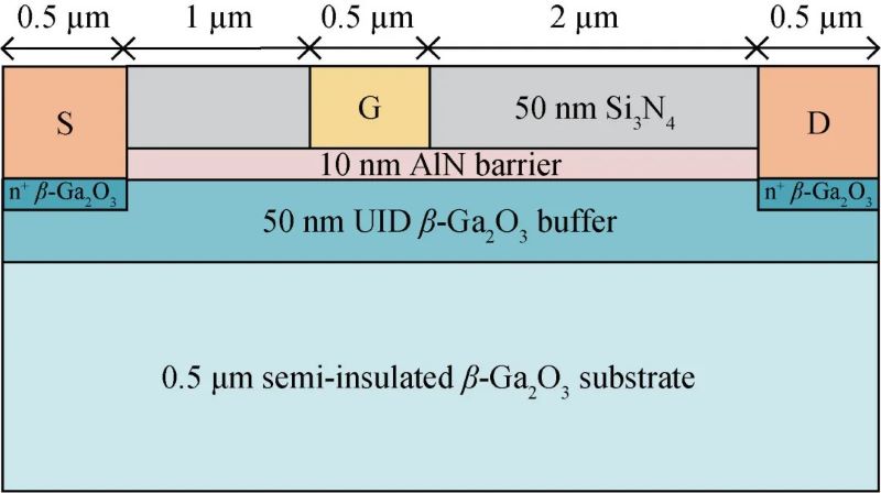
Figure 1. AlN/β-Ga2O3 HEMT structure diagram
AlN barrier layer thickness (tAlN) is an important structural parameter of HEMT devices, which has an effect on the band structure and 2DEG density of the devices. During the simulation, the drain-source voltage (VDS) is set to 15 V, and the tAlN is 10, 15, 20 and 25 nm, respectively. The device characteristics of different AlN barrier layer thicknesses are shown in Figure 2.
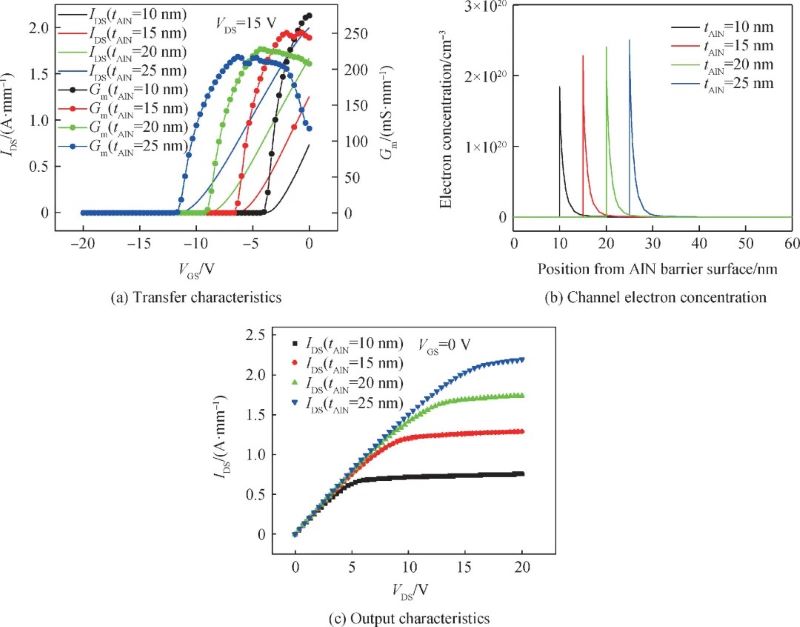
FIG. 2 Device characteristics of different AlN barrier thicknesses
From the transfer characteristic curve shown in Figure 2(a), it can be seen that when the barrier layer thickness is 10, 15, 20 and 25 nm, the threshold voltage of the device is -3.7, -6.3, -8.8 and -11.4V, respectively, indicating that with the increase of the thickness of the AlN barrier layer, the curve moves negatively and the threshold voltage decreases. As can be seen from Figure 2(b), the channel electron concentration continues to increase as the thickness of the AlN barrier layer increases. At the same time, it can be found from Figure 2(a) that the transconductance (Gm) changes with the thickness of the barrier layer, and the maximum transconductance is 271, 251, 228 and 217 mS/mm, respectively. With the increase of AlN barrier layer thickness, the maximum transconductance decreases, which indicates that the control ability of gate voltage on output current is weakened. It can be seen from the output characteristic curve in Figure 2(c) that when AlN thickness is 10, 15, 20 and 25 nm, the saturation leakage current (IDsat) is 0.8, 1.3, 1.8 and 2.2 A/mm, respectively. This indicates that with the increase of AlN thickness, the saturation leakage current increases. From the above analysis, it can be seen that even if AlN is undoped, the concentration of electron gas up to 1020 cm-3 can be formed on the β-Ga2O3 side of the AlN/β-Ga2O3 heterojunction. The energy sink depth and channel electron concentration at the interface of the heterojunction can be adjusted by adjusting the thickness of the AlN barrier layer, so as to achieve the regulation of the threshold voltage.
The influence of the gate length (lg) of AlN/β-Ga2O3 HEMT on the DC characteristics of the device is shown in Figure 3. In the simulation process, the drain-source voltage (VDS) is set to 15 V, and lg is respectively 0.1, 0.3, 0.5, 7.0 and 0.9 μm. At the same time, in order to keep the transverse size of the device unchanged, the gate drain spacing (lgd) corresponding to different gate lengths is 2.4, 2.2, 2.0, 1.8 and 1.6 μm respectively.

FIG. 3 Device characteristics of different gate lengths
From the output characteristic curve, when the gate length is 0. 9, 0. 7, 0. 5, 0. 3, 0. 1 μm, the on-resistance is 6. 8, 6. 6, 6. 4, 6. 2, 6. 0 Ω·mm respectively. The on-resistance decreases with the shortening of the gate length, which is caused by the increase of the electron concentration in the channel under the gate and the decrease of the gate resistance. It can also be seen from the output characteristic curve that when the gate length is long, the device saturation leakage current (IDsat) basically remains unchanged, but when the gate length is shortened to 0.1μm, the device drain saturation current increases with the increase of drain-source voltage (VDS). That is, the output conductance of the device increases with the shortening of the gate length, resulting in the deterioration of the saturation characteristics of the device, indicating that the device has a short channel effect.
The effect of gate position of AlN/β-Ga2O3 HEMT device on the DC characteristics of the device is shown in Figure 4. The fixed gate length is 0.3 μm, the drain-source voltage (VDS) is set to 15 V, the gate-drain spacing (lgd) is 1.7, 2.2 and 2.7 μm respectively, and the corresponding gate-source spacing (lgs) is 1.5, 1.0 and 0.5 μm respectively.
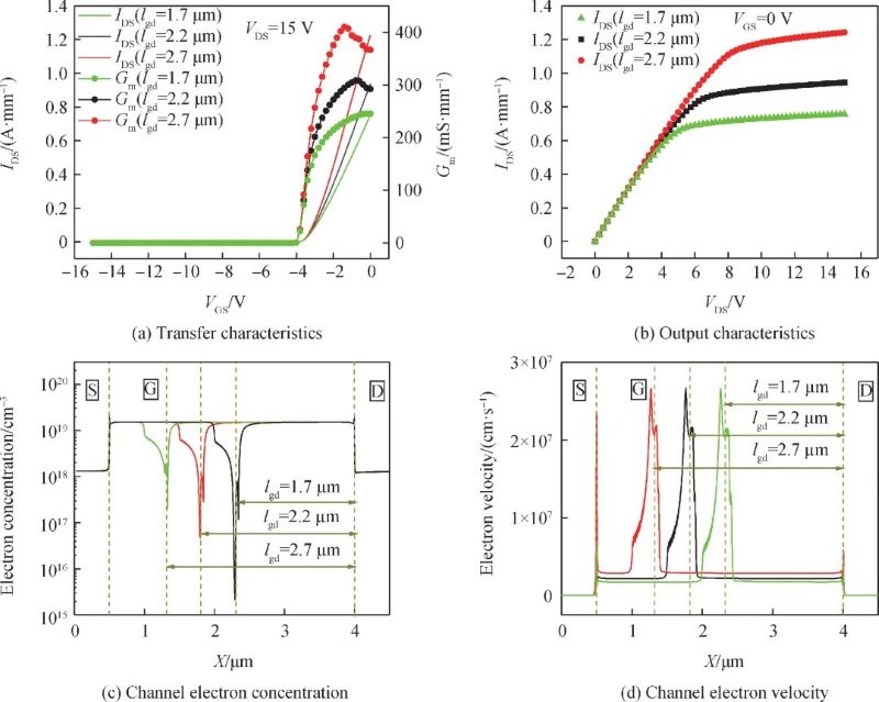
FIG. 4 Device characteristics with different gate drain spacing
As can be seen from the transfer characteristic curve in Figure 4(a), the threshold voltage for different gate drain spacing is -3.8V. The threshold voltage does not change with the change of grid-drain spacing. When the gate-source voltage (VGS) is set to 0 V and the gate-drain spacing (lgd) is 1.7, 2.2, 2.7 μm respectively, the output characteristics are shown in Figure 4(b). It can be seen from the output characteristic curve that when the gate drain spacing (lgd) is 1.7, 2.2 and 2.7 μm respectively, the saturation leakage current is 0.8, 0.9 and 1.2 A/mm respectively. The drain current of the device is proportional to the channel electron concentration and the channel electron velocity. With the increase of gate drain spacing, the electron concentration in the channel region does not change, while the electron velocity increases slightly, so the saturation drain current increases, as shown in Figure 4(c) and (d).
This section explores the influence of schottky gate metal type on the DC characteristics of the device by changing the work function (Wm) of the gate metal. Set the schottky gate metal work function to 5.15, 5.46 and 5.65 eV respectively, and the resulting device characteristics are shown in Figure 5.
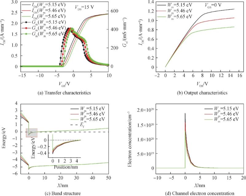
FIG. 5 Device characteristics of different gate metal work functions
As can be seen from the transfer characteristic curve in Figure 5(a), when the schottky gate metal work function is 5.15, 5.46, and 5.65 eV, the threshold voltages are -3.8, -3.3, and -2.8 V respectively. From the expression of the threshold voltage, it can be seen that the increase of the schottky gate metal work function will increase the threshold voltage. As can be seen from the output characteristic curve in Figure 5(b), when the schottky gate metal work function is 5.15, 5.46 and 5.65 eV respectively, the maximum saturation leakage current is 1.2, 1.0 and 0.8 A/mm respectively. When the schottky gate metal is in contact with the AlN barrier layer, because the Fermi level of the AlN barrier layer is higher than the Fermi level of the gate metal, the electrons in the AlN barrier layer will flow to the metal, making the surface of the AlN barrier layer positively charged and the metal surface negatively charged, forming an electric field from AlN to the metal and strengthening the polarized electric field. The greater the difference between the schottky gate metal and the AlN Fermi level, the stronger the electric field on the AlN surface, the greater the strengthening effect on polarization, and the greater the degree of tilt of the AlN band, as shown in Figure 5(c). The greater the band tilt, the smaller the donor-like surface state ionization degree, and the smaller the 2DEG concentration provided to the channel, as shown in Figure 5(d).
Conclusion
The surface density charge of AlN/β-Ga2O3 heterojunction is 2.75×1013 cm-2, which is the same order of magnitude as the 2DEG surface density of AlGaN/GaN HEMT devices. Then, the DC characteristics of AlN/β-Ga2O3 HEMT devices are studied. By electrical analysis of AlN barrier layer thickness, gate length, gate position and Schottky gate metal type, it is obtained that: The transconductance of the device increases with the increase of AlN barrier layer thickness, the decrease of gate length and the increase of gate-drain distance, in which the gate length has the greatest effect on it. With the increase of schottky gate metal work function, the threshold voltage of the device moves forward and the saturation leakage current decreases. The study of the influence of device structure parameters on device performance provides a theoretical basis for the design and improvement of subsequent devices.
