


Member News
【Member News】Hangzhou Fujia Gallium Industry Technology Co., LTD. ——Product Introduction
日期:2024-09-06阅读:1130
Hangzhou Fujia Gallium Industry Technology Co., Ltd. was established in December 2019. Its single crystal growth technology comes from Shanghai Institute of Optics and Fine Mechanics. The Crystal Materials Laboratory under the Institute has been conducting research on Gallium Oxide single crystal materials since 2004, and is the first team to carry out research on the growth technology of Gallium Oxide single crystal materials in China. By 2024, our company has obtained 50 authorized domestic and international patents, and won the honor of "National High-tech Enterprise" and "Zhejiang Province Specialized and special new small and medium enterprises". Fujia adheres to the production of high-quality Gallium Oxide single crystal materials as its core business and continues to expand upstream and downstream. While providing high-quality and cost-effective Gallium Oxide single crystal substrates and epitaxial wafers to epitaxy and device customers, Fujia is also providing its peers in the field of Gallium Oxide materials with technology-verified Gallium Oxide single crystal growth furnace, Gallium Oxide single crystal substrate polishing equipment. Contribute to the development of Gallium Oxide industry.
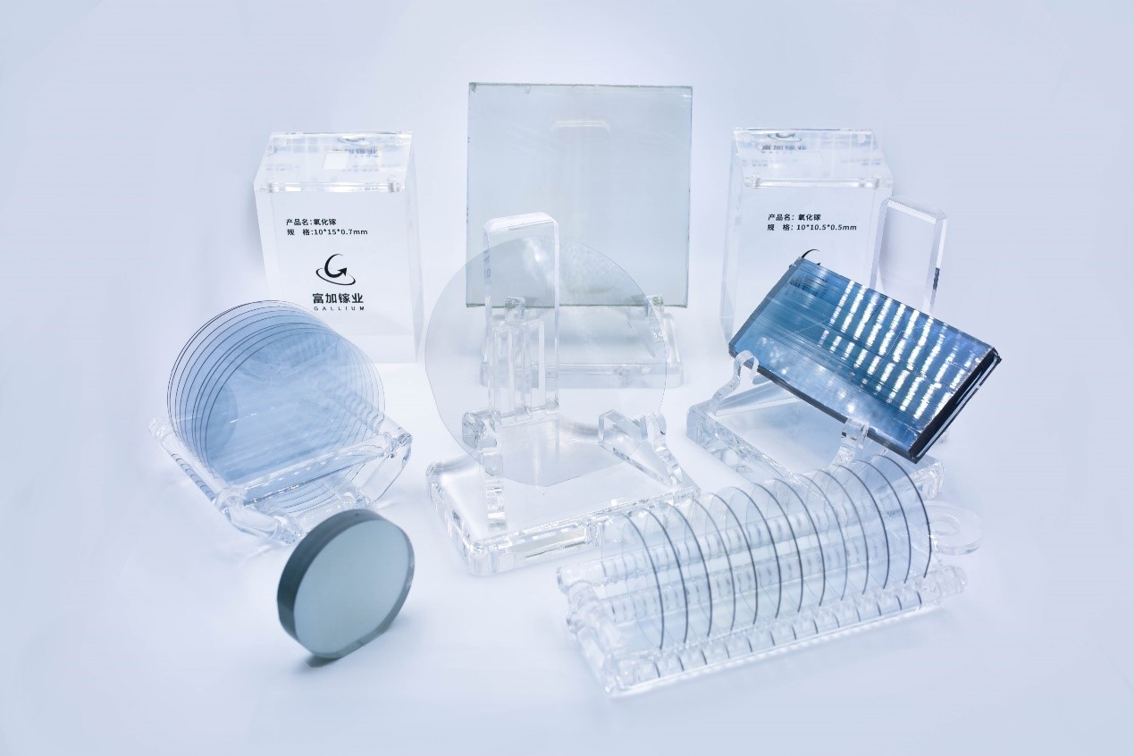
In recent years, our company has continuously improved the Gallium Oxide single crystal processing technology, overcome the technical problems of 6-inch Gallium Oxide single crystal substrate and ultra-thin substrate processing, and introduced to the market the (100) and (001) ultra-thin substrate in addition to the standard thickness products, which is more conducive to solving the problem of low thermal conductivity of Gallium Oxide single crystal material, and improve the heat dissipation capacity of the device. To provide more options for R&D personnel.
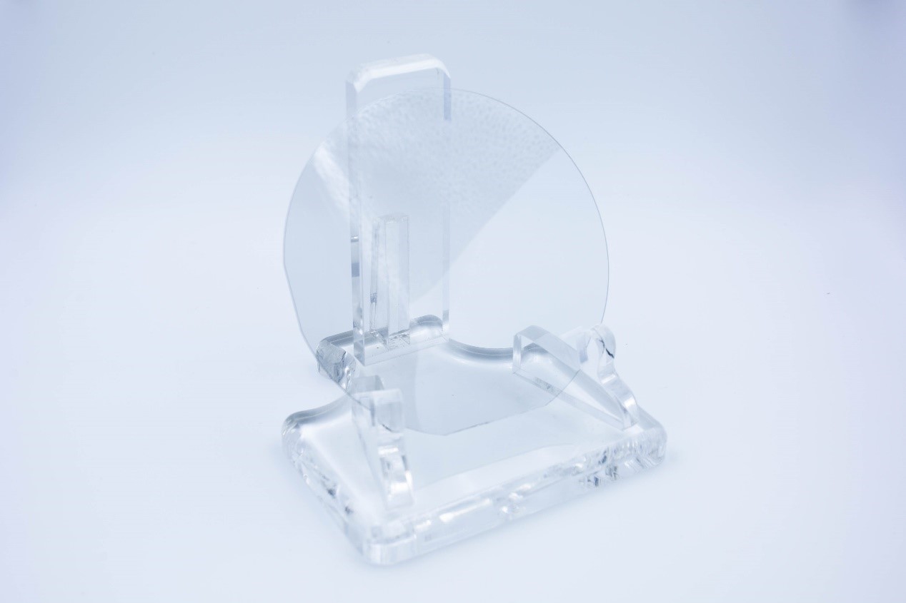
Figure 2: 6-inch Gallium Oxide Wafers
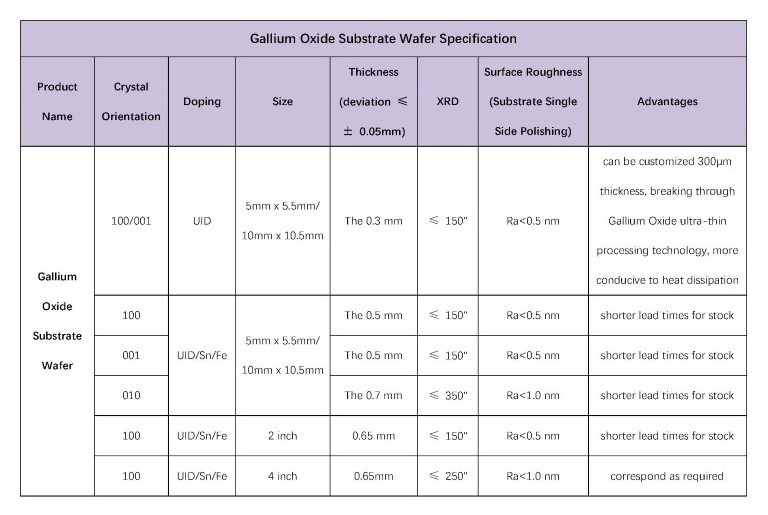
The list of product specifications for Gallium Oxide substrates on sale is as follows:
In addition, the company broke through the technical problems of high-quality processing of hard and brittle materials, achieved efficient cutting of Gallium Oxide wafers, and cut small-size Gallium Oxide wafer from 2-inch and 4-inch standard wafers, greatly improving the performance consistency of Gallium Oxide wafer, and further reducing the price of Gallium Oxide wafer, providing consistent and cost-effective products for downstream customers.
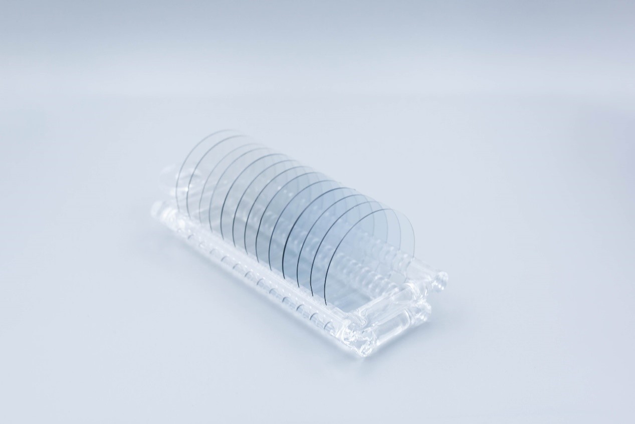
Figure 4: 2 inch Gallium Oxide Wafer
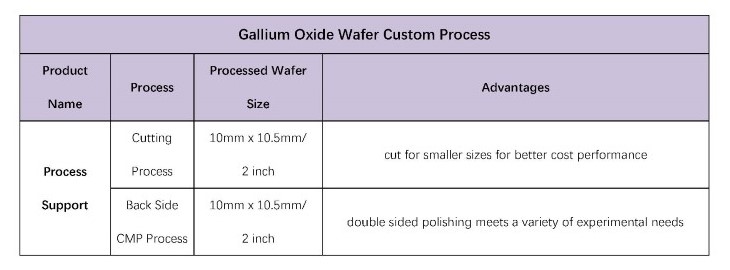
The list of Gallium Oxide custom process services is as follows:
While developing Gallium Oxide substrate, the company is also simultaneously carrying out the layout of Gallium Oxide homogeneous epitaxy, including MBE and MOCVD homogeneous epitaxy technical routes, to solve the current international embargo of MBE epitaxy materials in the field of Gallium Oxide in China and the uniformity problem of homogeneity of HVPE epitaxy films. Through the series of key technical research, it has been possible to provide a stable supply of high quality standard MBE epitaxial wafer, and to break the international blockade of MBE epitaxial wafer in our country. At the same time, the Gallium Oxide homogeneous epitaxial wafer products based on MOCVD technology have entered the comprehensive evaluation stage and are about to enter the market.
Figure 6: Gallium Oxide MBE Epitaxial Wafer
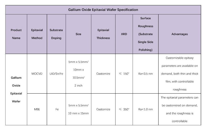
The list of product specifications of Gallium Oxide epitaxial wafer for sale is as follows:
At the same time, our company can provide scientific research grade Gallium Oxide substrate and epitaxial wafer according to demand, which is more suitable for the initial research and development or process verification work, greatly reducing the early research and development cost.
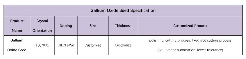
In order to further promote the development of Gallium Oxide industry, since August 2024, our company has provided high-quality standard seed products and customized seed crystals to the market, allowing more teams dedicated to the research of wide band gap semiconductor new materials to enter the field of Gallium Oxide smoothly.
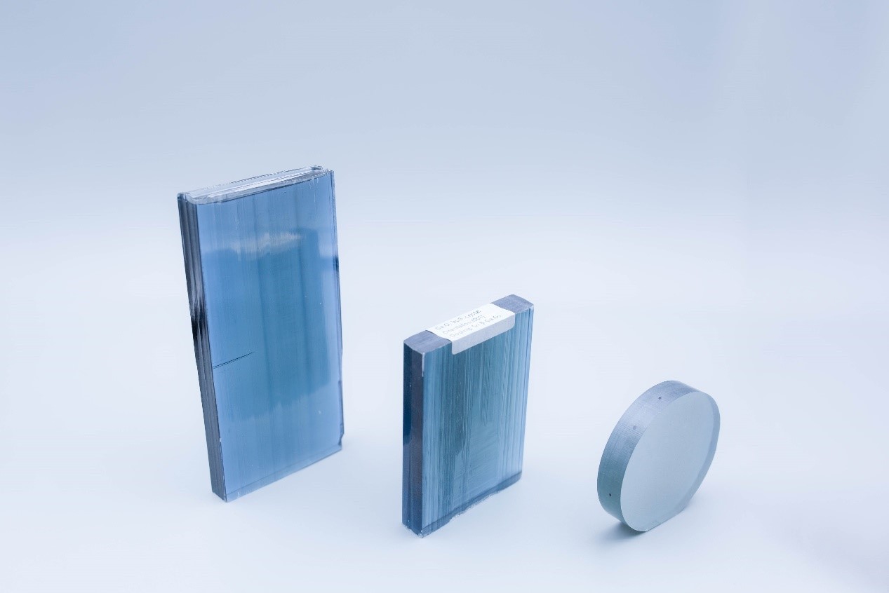
Figure 8: Gallium Oxide Ingot
The list of Gallium Oxide seed product specifications is as follows:
Welcome to inquire
Contact Window:
Ms. Guo (13164023887)
Ms. Sun (15757190545)
