Paper Sharing
【Domestic Papers】Synthesis of InAl-alloyed Ga₂O₃ nanowires for self-powered ultraviolet detectors by a CVD method
日期:2024-09-20阅读:993
Researchers from the Chongqing University of Technology have published a dissertation titled "Synthesis of InAl-alloyed Ga2O3 nanowires for self-powered ultraviolet detectors by a CVD method" in RSC Advances.
Abstract
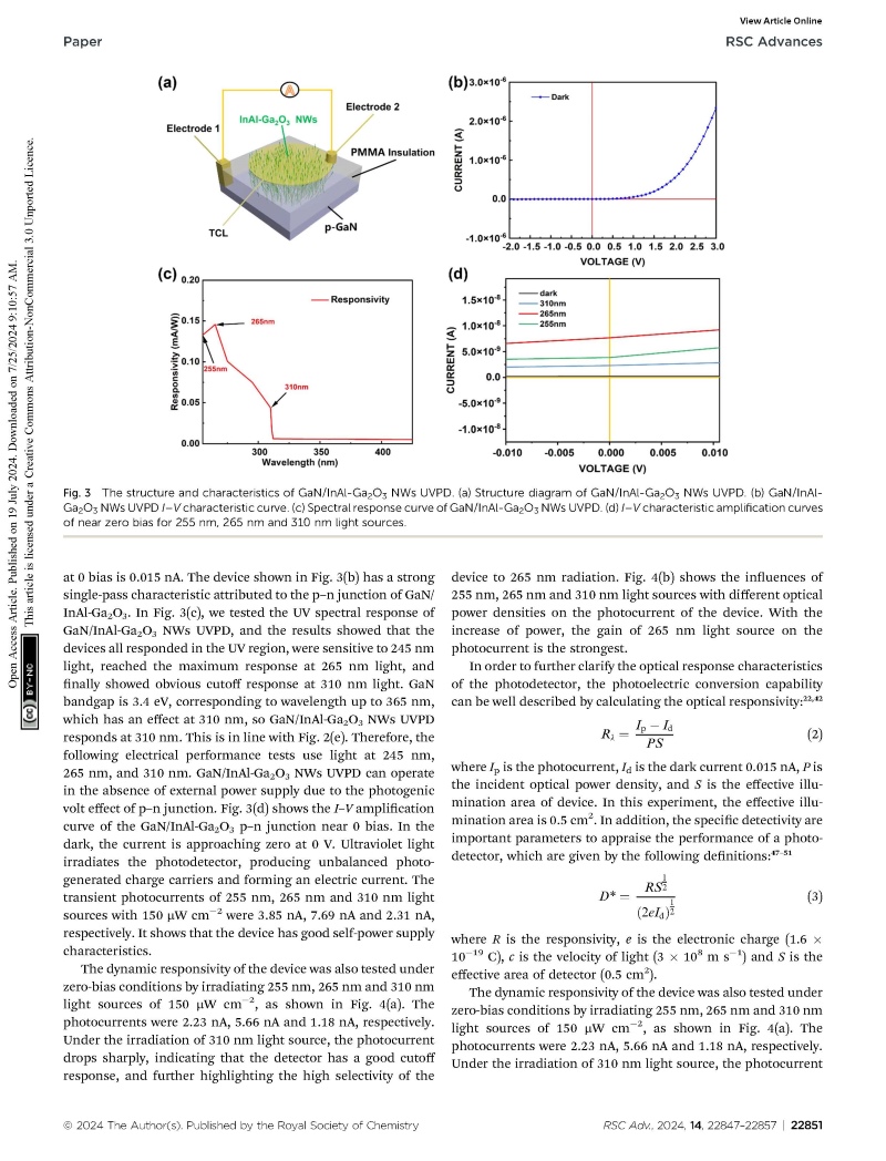
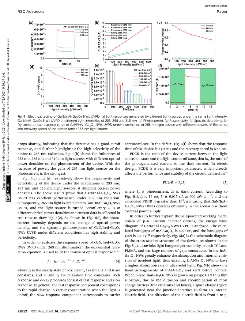
Ga2O3 is a kind of wide-band gap semiconductor, which has great potential in deep ultraviolet detection because of its high efficiency and fast response. Doping can improve the photoelectric properties of Ga2O3 materials. In this paper, In and Al elements alloyed Ga2O3 nanowires (InAl-Ga2O3 NWs) were successfully grown on p-GaN using a cost-effective chemical vapor deposition method and a vertical structure. The GaN/InAl-Ga2O3 NWs p–n self-powered wide-gap UV photodetector (PD) was constructed based on sputtered gold film as the bottom and top electrodes, and spin coated with polymethyl methacrylate as the insulating layer in the vertical direction. The GaN/InAl-Ga2O3 UV PD exhibits excellent performances, including an extremely low dark current of 0.015 nA, a maximum photocurrent of about 16 nA at zero-bias voltage under 265 nm illumination, and a light-to-dark current ratio greater than 103. The responsivity is 0.94 mA W−1, the specific detectivity is 9.63 × 10⁹ jones, and the good fast response/attenuation time is 31.2/69.6 ms. The self-powered characteristics are derived from the internal electric field formed between p-type GaN and n-type InAl-Ga2O3 NWs, which is conducive to the rapid separation and transfer of photogenerated carriers. This work provides an innovative mechanism of high-performance metal oxide nanowires for the application of p–n junction photodetectors, which can operate without any external bias.
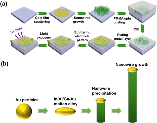
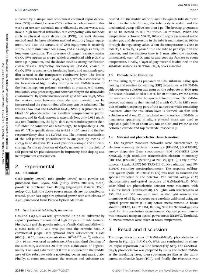
Fig. 1 Process schematic diagram. (a) Preparation process flow chart. (b) Schematic diagram of InAl-Ga2O3 NWs growth principle.
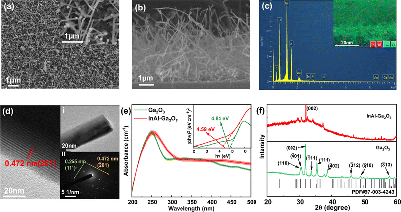
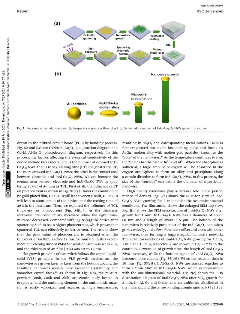
Fig. 2 Characterization of material properties. (a) InAl-Ga2O3 NWs SEM top view and (b) sectional diagrams. (c) EDS spectra. The illustration is the distribution of elements. (d) InAl-Ga2O3 NWs TEM images, the inset HRTEM pictures and SAED patterns. (e) Ultraviolet absorption spectra of InAl-Ga2O3 NWs and Ga2O3 NWs deposited on Al2O3 substrate. The inset are Tauc plots according to Kubelka–Munk function of InAl-Ga2O3 NWs, Ga2O3 NWs. (f) XRD patterns of InAl-Ga2O3 NWs and Ga2O3 NWs.
DOI:https://doi.org/10.1039/D4RA04176C