Paper Sharing
【International Papers】Deep Level Traps in (010) β-Ga₂O₃ Epilayers Grown by Metal Organic Chemical Vapor Deposition on Sn-Doped β-Ga₂O₃ Substrates
日期:2024-10-24阅读:897
Researchers from the The University of Manchester have published a dissertation titled "Deep level traps in (010) β-Ga2O3 epilayers grown by metal organic chemical vapor deposition on Sn-doped β-Ga2O3 substrates " in Journal of Applied Physics.
ABSTRACT
In this work, conventional deep-level transient spectroscopy (DLTS) and high-resolution Laplace-DLTS (L-DLTS) have been used to characterize deep-level traps in (010) β-Ga2O3 epilayers grown by metal organic chemical vapor deposition on native Sn-doped substrates. Two types of epilayers have been studied, one doped with silicon during growth to about 1.5 × 1017 cm−3 and the other type was unintentionally doped (UID). Electrical measurements were conducted on Au and Pt Schottky barrier diodes. In the Si-doped samples, only one electron trap with emission activation energy of 0.42 eV (E0.42) and concentration of (6–8) × 1013 cm−3 has been detected. In the UID samples, in addition to the E0.42 trap, two other traps with activation energies for electron emission of 0.10 eV (E0.10) and 0.53 eV (E0.53) have been observed. Dependencies of electron emission rate (eem) on the electric field (E) as well as concentration-depth profiles {NT(W)} have been measured and analyzed for the E0.10 and E0.42 traps. The eem(E) dependence for the E0.10 trap is characteristic for a donor energy level, while that for the E0.42 trap indicates an acceptor level. The NT(W) dependencies show non-uniform spatial distributions of both the E0.10 and E0.42 traps in the UID samples, with the concentration of the E0.10 trap dropping from about 1 × 1015 cm−3 at 1.5 μm from the surface to about 2 × 1013 cm−3 at 0.5 μm, which indicates out-diffusion from the substrate or interface into the epilayer as a likely source. The results obtained are compared with the literature, and possible origins of the detected traps are discussed.
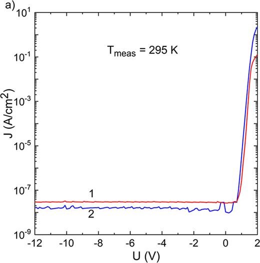
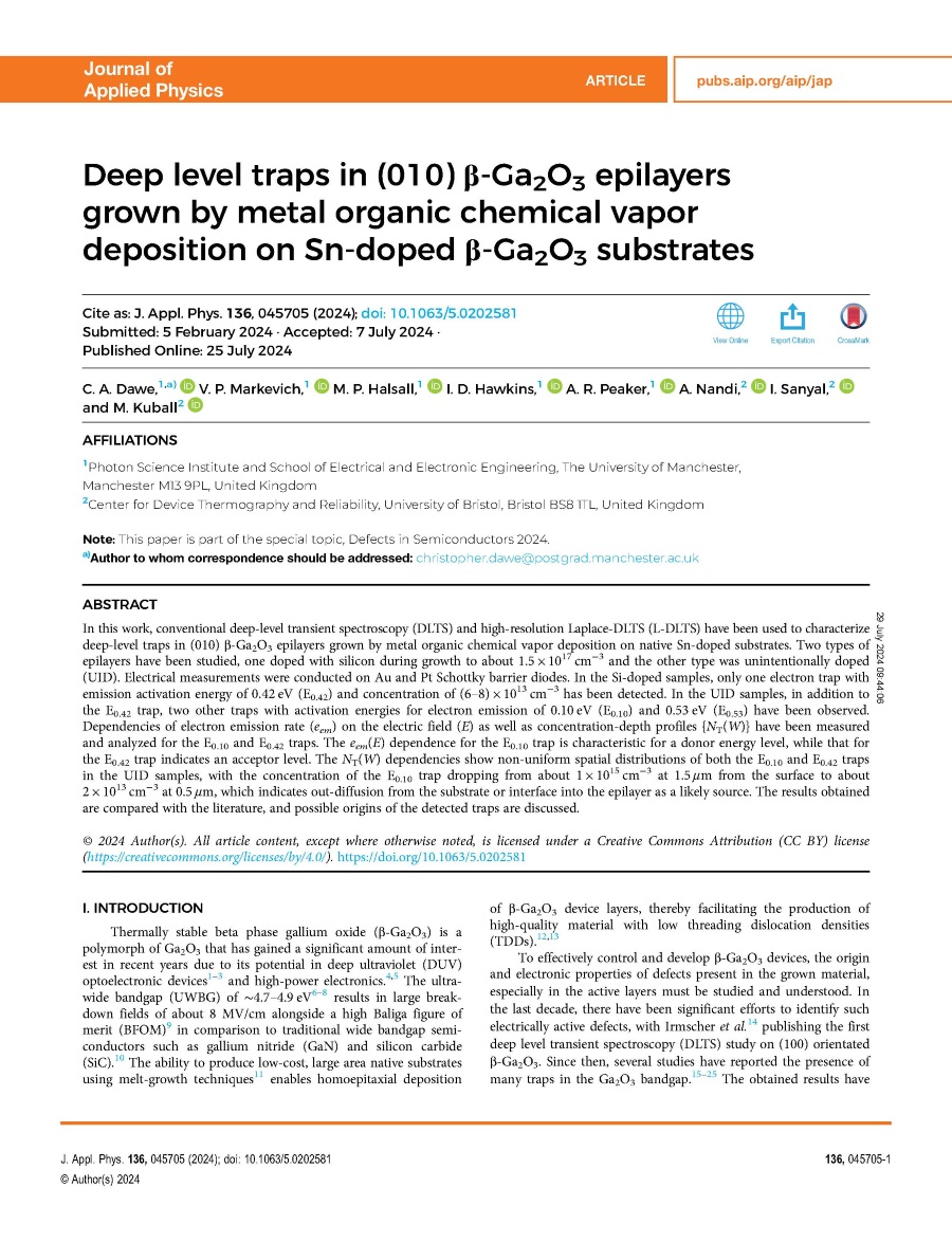
FIG. 1. Current density–voltage (J–V) dependencies for the Au Schottky diodes on the Si-doped (red curve) and the UID (blue curve) epilayers, measured at 295 K.

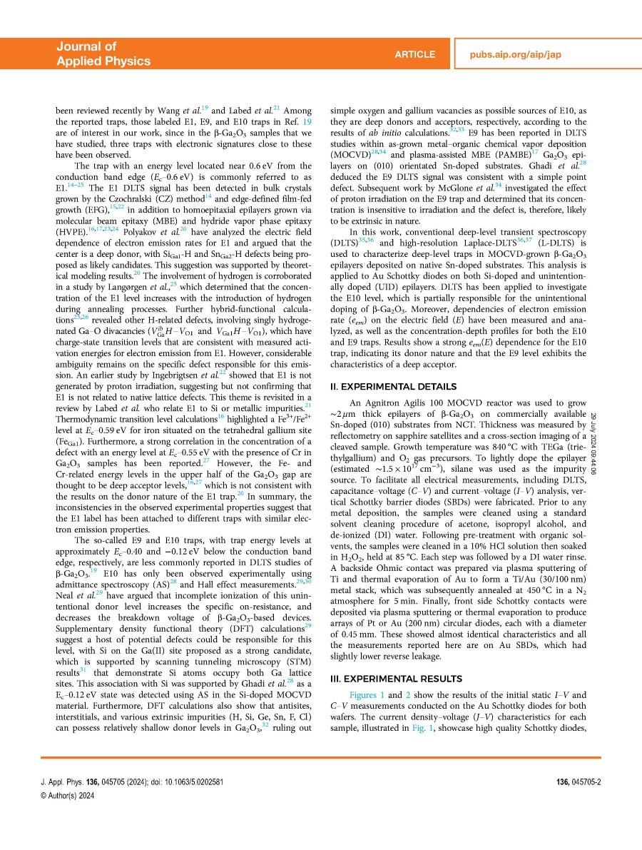
FIG. 2. (a) 1/Cb2 dependencies on the applied reverse bias and (b) spatial profile of the uncompensated donors [Nd (W)] for the Au Schottky diodes on the Si-doped (red curves) and UID (blue curves) epilayers. Results are derived from capacitance–voltage (C–V) measurements conducted at 295 K.
DOI:
https://doi.org/10.1063/5.0202581