


Member News
【Member News】Breakthrough Progress in Fujia Gallium——Gallium Oxide Epitaxial Wafer Completes MOSFET Lateral Power Device Verification
日期:2024-10-31阅读:1277
At the same time that domestic and international colleagues focus on the development of single-crystal materials, Hangzhou Fujia Gallium Technology Co., LTD. (hereinafter referred to as Fujia Gallium) has advanced the layout of epitaxy technology. Supported by the National Key R&D Program "Research on Large-Size Gallium Oxide Semiconductor Materials and High-Performance Devices" (Project No.: 2022YFB3605500), they developed a high-performance MBE epitaxial wafer, and cooperated with the device team of the National Key R&D Program, successfully prepared a MOSFET lateral power device with a breakdown voltage greater than 2000 V and a current density of 60 mA/mm, which is comparable to the performance of the imported epitaxial wafer prepared devices.
Fujia Gallium provides Gallium Oxide epitaxial wafer prepared by Molecular Beam Epitaxy (MBE) technology, which adopts a double-layer epitaxy structure is composed of an unintentional doping layer and a Sn doping layer. The substrate material is semi-insulated (010) Fe doped Gallium Oxide, which is mainly used in lateral power devices. The carrier concentration of the doped layer of conventional products is 1-4E17 cm-3, the mobility is > 80 cm2/V·s, and the surface roughness is < 2 nm.
The device team of the National Key R&D Program conducted preliminary wafer verification on the MBE Gallium Oxide epitaxial wafer product. The current density of the 12μm drain-gate space Gallium Oxide MOSFET device is 60 mA/mm (FIG. a), the specific on-resistance is about 42 mΩ∙cm2, and the breakdown voltage can reach 2242 V (FIG. b). The device performance is comparable to that of imported similar materials. Fujia Gallium will continue to improve and optimize the epitaxial products according to the feedback results of device development, and is committed to providing stable and controllable high-quality Gallium Oxide single crystal substrate and epitaxial products for downstream device manufacturers, providing material support for China to build an internationally competitive Gallium Oxide industry chain, and realizing the full link connectivity of Chinese Gallium Oxide based devices.
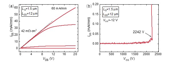
Figure a-b DC output characteristic curve and breakdown voltage curve of a Gallium Oxide MOSFET with drain-gate space LG=12 μm and gate length L=1.5 μm
About Fujia Gallium
Hangzhou Fujia Gallium Technology Co., LTD., founded on December 31, 2019, is the first "hard technology" enterprise registered by Hangzhou Institute of Optics and Fine Mechanics. With the vision of "Making the World Use Good Materials", the company focuses on the industrialization work of wide bandgap semiconductor Gallium Oxide materials. Mainly engaged in the growth of Gallium Oxide single crystal materials, Gallium Oxide substrate and epitaxial wafer research and development, production and sales, the products are mainly used in power devices, microwave radio frequency and photoelectric detection fields.
At present, the company has won a number of honors: In 2022, it won the Zhejiang Province Science and Technology Small and Medium-Sized Enterprise; National High-Tech Enterprise in 2023; In 2024, it will be awarded as Hangzhou Enterprise High-Tech Research and Development Center and Zhejiang Special Small and Medium-Sized Enterprise. It undertook one Gallium Oxide project for the National Development and Reform Commission and participated in three national and provincial projects from the Ministry of Science and Technology, Zhejiang Province, and Shanghai. In addition, it has obtained 12 international patents authorized (6 in the United States and 6 in Japan), 40 domestic patents authorized, 3 trademark certification and registration of "Fujia Gallium Industry", and 3 software copyrights (crystal growth control software).
For more information about Hangzhou Fujia and its products
Please visit our official website: www.fujia-hiom.com
