


Paper Sharing
【Domestic Papers】Sun Huarui’s Team from Harbin Institute of Technology: Three-Dimensional Thermal Analysis of Heterogeneously Integrated β-Ga₂O₃-on-SiC SBDs Using Raman Thermography and Electrothermal Modeling
日期:2024-11-06阅读:913

Recently, Professor Sun Huarui's team at Harbin Institute of Technology (Shenzhen) and Ou Xin's team of researchers at Shanghai Institute of Microsystem and Information Technology have made progress in the three-dimensional thermal analysis of heterogeneously integrated β-Ga2O3-on-SiC SBDs using Raman thermography and electrothermal modeling. The research results are entitled "Three-dimensional thermal analysis of heterogeneously integrated β-Ga2O3-on-SiC SBDs using Raman thermography and electrothermal modeling" was published in the international top journals of Applied Physics Letters. The paper was selected as an "Editor's Pick" article, which means that the work is of high academic value and is highly representative in the relevant field. Xie Yinfei, Ph.D., from Harbin Institute of Technology, Shenzhen (first author affiliation), and Xu Wenhui, Assistant Researcher from Shanghai Institute of Microsystems and Information Technology, are co-first authors of the paper, and Professor Sun Huarui and Researcher Ou Xin are co-corresponding authors.
β-Ga2O3 shows great potential in high-power electronics applications due to its ultra-wide bandgap and excellent electrical properties. However, β-Ga2O3 has intrinsic low thermal conductivity, and in order to meet the needs of high power density applications, researchers have explored heterogeneous integration of β- Ga2O3 with high thermal conductivity substrates such as SiC in recent years. In order to evaluate the heat dissipation performance of new heterogeneous integration Gallium Oxide devices, it is necessary to conduct a comprehensive analysis of their temperature distribution and thermal resistance composition under operating conditions. Traditional temperature measurement methods such as thermocouple, electrical pulse method, infrared thermal imaging, etc., are challenging to accurately measure the channel temperature of β- Ga2O3-based devices due to their damage or lack of spatial resolution, and the transparency of ultra-wide bandgap semiconductor materials to infrared spectra.
This study employs three-dimensional Raman thermography to investigate the thermal properties of β-Ga2O3-on-SiC (GaOISiC) and β- Ga2O3 bulk Schottky Barrier Diodes (SBDs) at various input power levels. The peak temperature and the spatial distribution of temperature along channel and cross-depth of β- Ga2O3 based devices were accurately characterized. In this study, Raman measuring points are evenly distributed between the anode and cathode to analyze the horizontal temperature distribution of the device. The laser beam is focused at different depths inside the device for temperature depth scanning. For heterogeneous integration GaOISiC SBD, because the transferred β-Ga2O3 layer is very thin (~130 nm), the near-surface junction temperature can be directly measured by Raman in this study. For β-Ga2O3 bulk SBD, the average temperature at a certain depth detected by Raman spectra is lower than the junction temperature near the surface. Therefore, in this study, the Raman enhancement technique of nanoparticles is used to measure the surface temperature of the device. Figure 1 (a, b) compares the temperature distribution along the lateral and depth directions near the peak temperature point. The results show significant heating in the channel near the internal electrode, especially for the transverse circular SBD with an internal anode showing significant heat accumulation, which is attributed to the higher current density and increased resistance of the anode's Schottky contact. Figure 1 (c) compares the peak temperature rise and thermal resistance of the two SBDs under different input power under three different methods: Raman thermal imaging, three-dimensional electrothermal simulation using Technology Computer-Aided Design (TCAD) and infrared thermal imaging. The results show that Raman thermal imaging is consistently closer to the TCAD simulation results than the temperature measured by the infrared camera, verifying the accuracy of the Raman temperature mapping, and the thermal resistance of the GaOISiC SBD is only one-third of that of the β-Ga2O3 bulk SBD. This study highlights the advantages of Raman thermal imaging combined with electrothermal simulation in accurately measuring the temperature of β-Ga2O3 based devices, which helps to visualize the three-dimensional heat dissipation path, and demonstrates the significant effect of heterogeneous integration in improving heat dissipation.
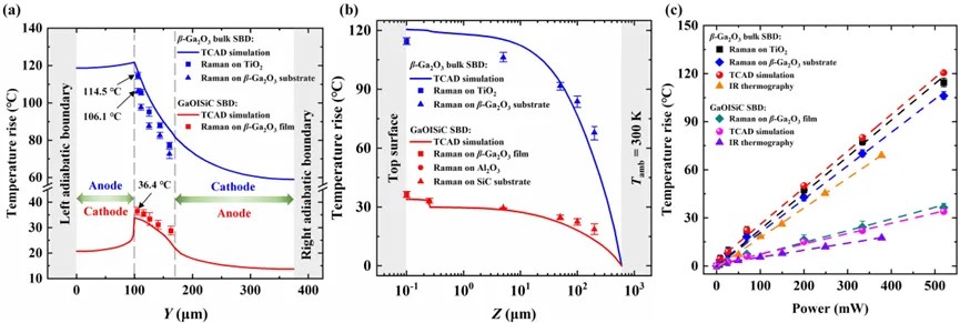
Figure 1 Temperature distribution in (a) transverse and (b) depth directions in the GaOISiC SBD and β-Ga2O3 bulk SBD, as well as (c) comparison of thermal resistance measured by different temperature measurement methods
DOI:
https://doi.org/10.1063/5.0208975
