Paper Sharing
【International Papers】Advanced defect spectroscopy in wide-bandgap semiconductors: review and recent results
日期:2024-11-15阅读:1052
Researchers from the University of Padova have published a dissertation titled "Advanced defect spectroscopy in wide-bandgap semiconductors: review and recent results" in Journal of Physics D: Applied Physics.
Abstract
The study of deep-level defects in semiconductors has always played a strategic role in the development of electronic and optoelectronic devices. Deep levels have a strong impact on many of the device properties, including efficiency, stability, and reliability, because they can drive several physical processes. Despite the advancements in crystal growth, wide- and ultrawide-bandgap semiconductors (such as gallium nitride and gallium oxide) are still strongly affected by the formation of defects that, in general, can act as carrier traps or generation-recombination centers (G-R). Conventional techniques used for deep-level analysis in silicon need to be adapted for identifying and characterizing defects in wide-bandgap materials. This topical review paper presents an overview of reviews of the theory of deep levels in semiconductors; in addition, we present a review and original results on the application, limits, and perspectives of two widely adopted common deep-level detection techniques, namely capacitance deep-level transient spectroscopy and deep-level optical spectroscopy, with specific focus on wide-bandgap semiconductors. Finally, the most common traps of GaN and β-Ga2O3 are reviewed.
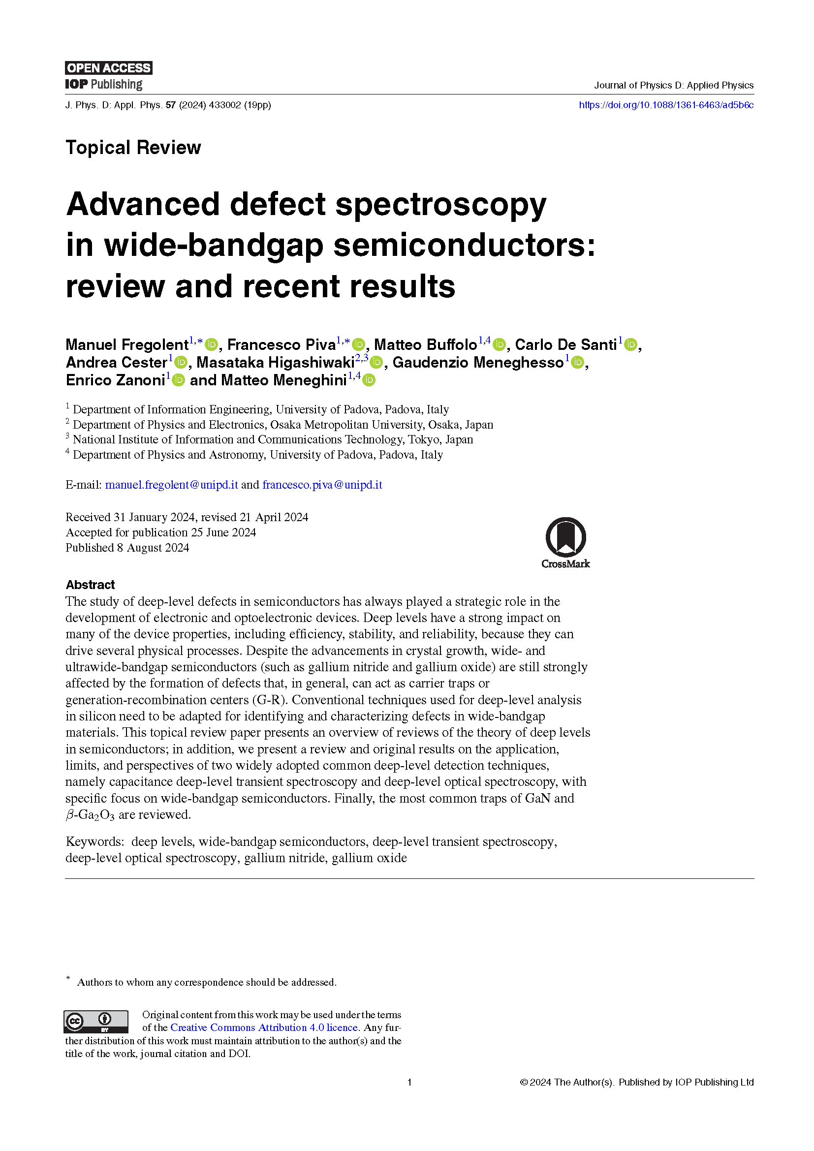
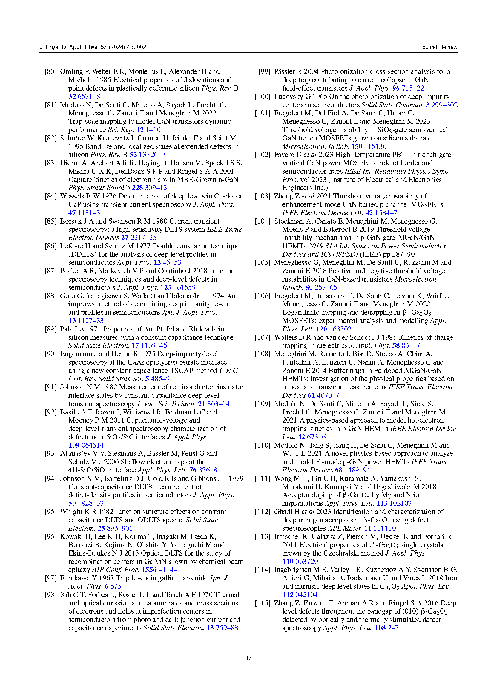
Figure 1. Perspective power, RF, and optoelectronics applications of wide-bandgap semiconductors GaN and β-Ga2O3.
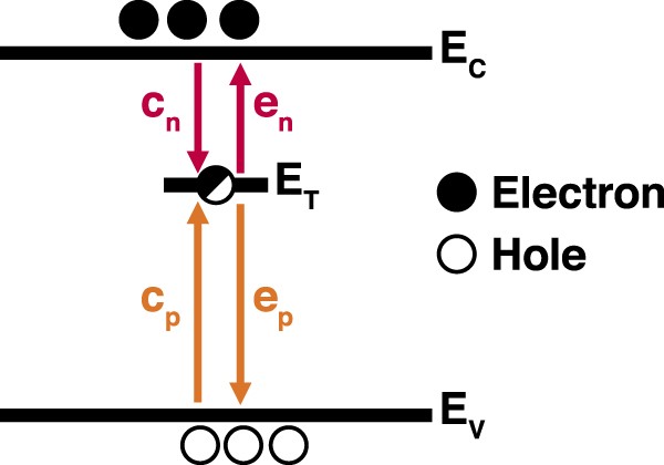
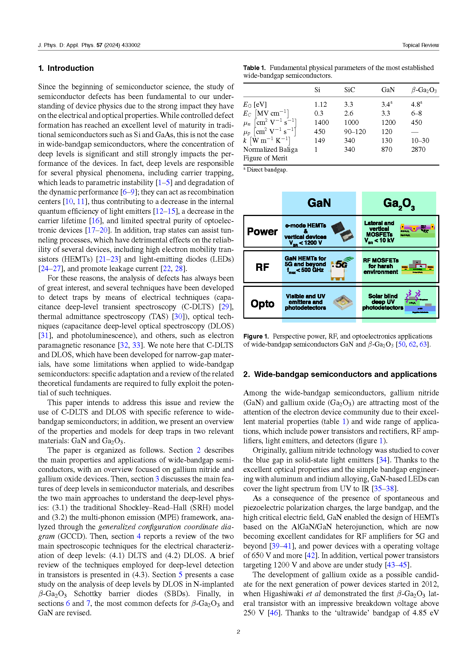
Figure 2. SRH model of the dynamic interaction between carriers and trap states. The four processes allowed by the model are described by the capture and emission coefficients cn, cp, en, ep.
DOI:
doi.org/10.1088/1361-6463/ad5b6c