Paper Sharing
【Domestic Papers】Researchers from Jilin University have developed improved-performance amorphous Ga₂O₃ photodetectors fabricated using capacitive coupled plasma-assisted magnetron sputtering
日期:2024-11-27阅读:982
Researchers from the Jilin University have published a dissertation titled "Improved-Performance Amorphous Ga2O3 Photodetectors Fabricated by Capacitive Coupled Plasma-Assistant Magnetron Sputtering" in Coatings.
Abstract
Ga2O3 has received increasing interest for its potential in various applications relating to solar-blind photodetectors. However, attaining a balanced performance with Ga2O3-based photodetectors presents a challenge due to the intrinsic conductive mechanism of Ga2O3 films. In this work, we fabricated amorphous Ga2O3 (a-Ga2O3) metal–semiconductor–metal photodetectors through capacitive coupled plasma assisted magnetron sputtering at room temperature. Substantial enhancement in the responsivity is attained by regulating the capacitance-coupled plasma power during the deposition of a-Ga2O3. The proposed plasma energy generated by capacitive coupled plasma (CCP) effectively improved the disorder of amorphous Ga2O3 films. The results of X-ray photoelectron spectroscopy (XPS) and current-voltage tests demonstrate that the additional plasma introduced during the sputtering effectively adjust the concentration of oxygen vacancy effectively, exhibiting a trade-off effect on the performance of a-Ga2O3 photodetectors. The best overall performance of a-Ga2O3 photodetectors exhibits a high responsivity of 30.59 A/W, a low dark current of 4.18 × 10⁻¹¹, and a decay time of 0.12 s. Our results demonstrate that the introduction of capacitive coupled plasma during deposition could be a potential approach for modifying the performance of photodetectors.
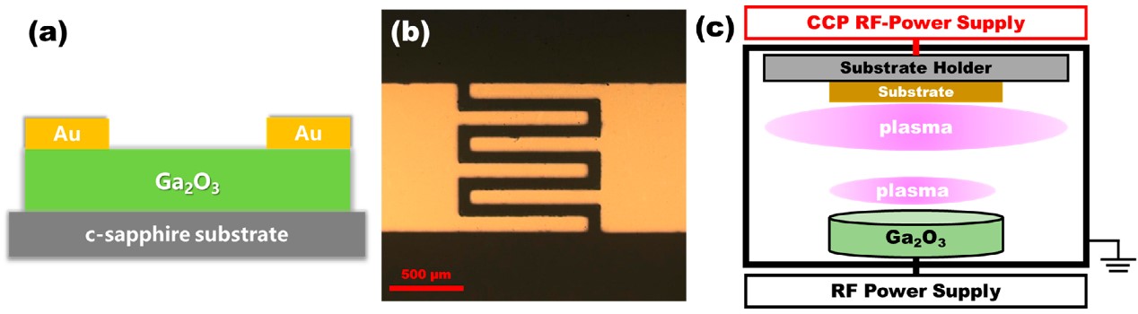
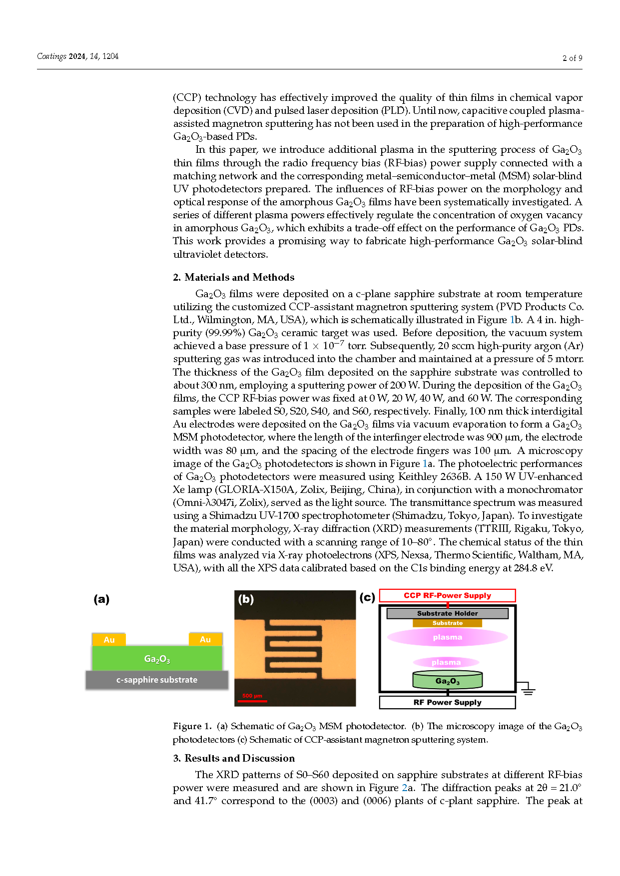
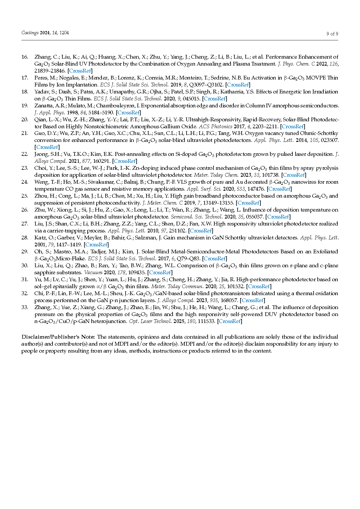
Figure 1. (a) Schematic of Ga2O3 MSM photodetector. (b) The microscopy image of the Ga2O3 photodetectors (c) Schematic of CCP-assistant magnetron sputtering system.
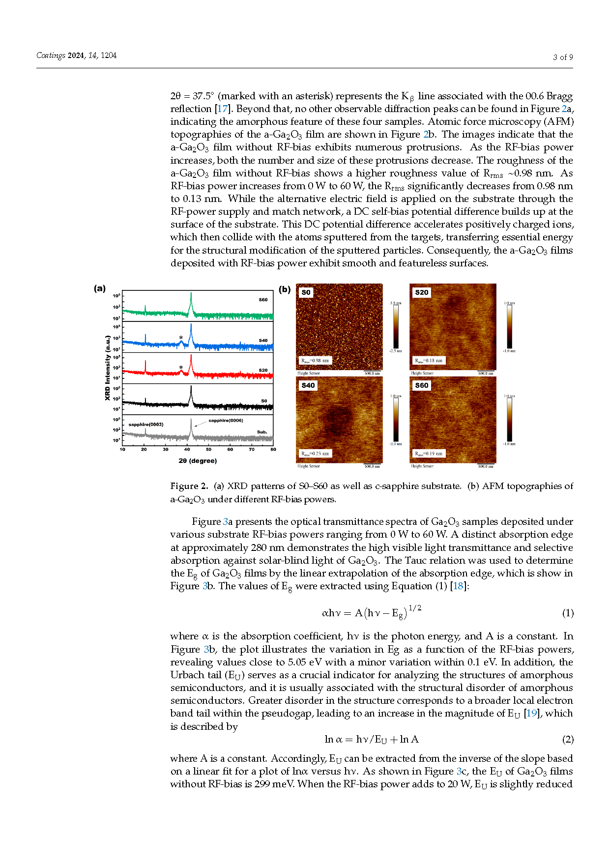
Figure 2. (a) XRD patterns of S0–S60 as well as c-sapphire substrate. (b) AFM topographies of a-Ga2O3 under different RF-bias powers.
DOI:
https://doi.org/10.3390/coatings14091204