Paper Sharing
【Member Papers】Researchers from the National Yang Ming Chiao Tung University investigated a hBN/ Ga₂O₃ pn junction diode
日期:2024-12-05阅读:7004
Researchers from the National Yang Ming Chiao Tung University have published a dissertation titled "A hBN/Ga2O3 pn junction diode" in Scientific Reports.
Abstract
The development of next-generation materials such as hBN and Ga2O3 remains a topic of intense focus owing to their suitability for efficient deep ultraviolet (DUV) emission and power electronic applications. In this study, we combine p-type hBN and n-type Ga2O3, forming a pseudo-vertical pn hBN/Ga2O3 heterojunction device. Rectification ratios > 105 (300 K) and ∼400 (475 K) are observed and are amongst the highest values reported to date for ultra-thin hBN-based pn junctions. The measured current under forward bias is ~2 mA, which we attribute to the shallow Mg acceptor level (60 meV), and 0.2 µA at −10 V. Critically, device performance remains stable and highly repeatable after a multitude of temperature ramps to 475 K. Capacitance-voltage measurements indicate widening the depletion region under increasing reverse bias voltage and a built-in voltage of 2.34 V is recorded. The hBN p-type characteristic is confirmed by Hall effect, a hole concentration of 7×1017 cm−3 and mobility of 24.8 cm2/Vs is achieved. Mg doped hBN resistance reduces by >108 compared to intrinsic material. Future work shall focus on the optical emission properties of this material system.
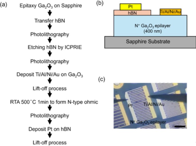
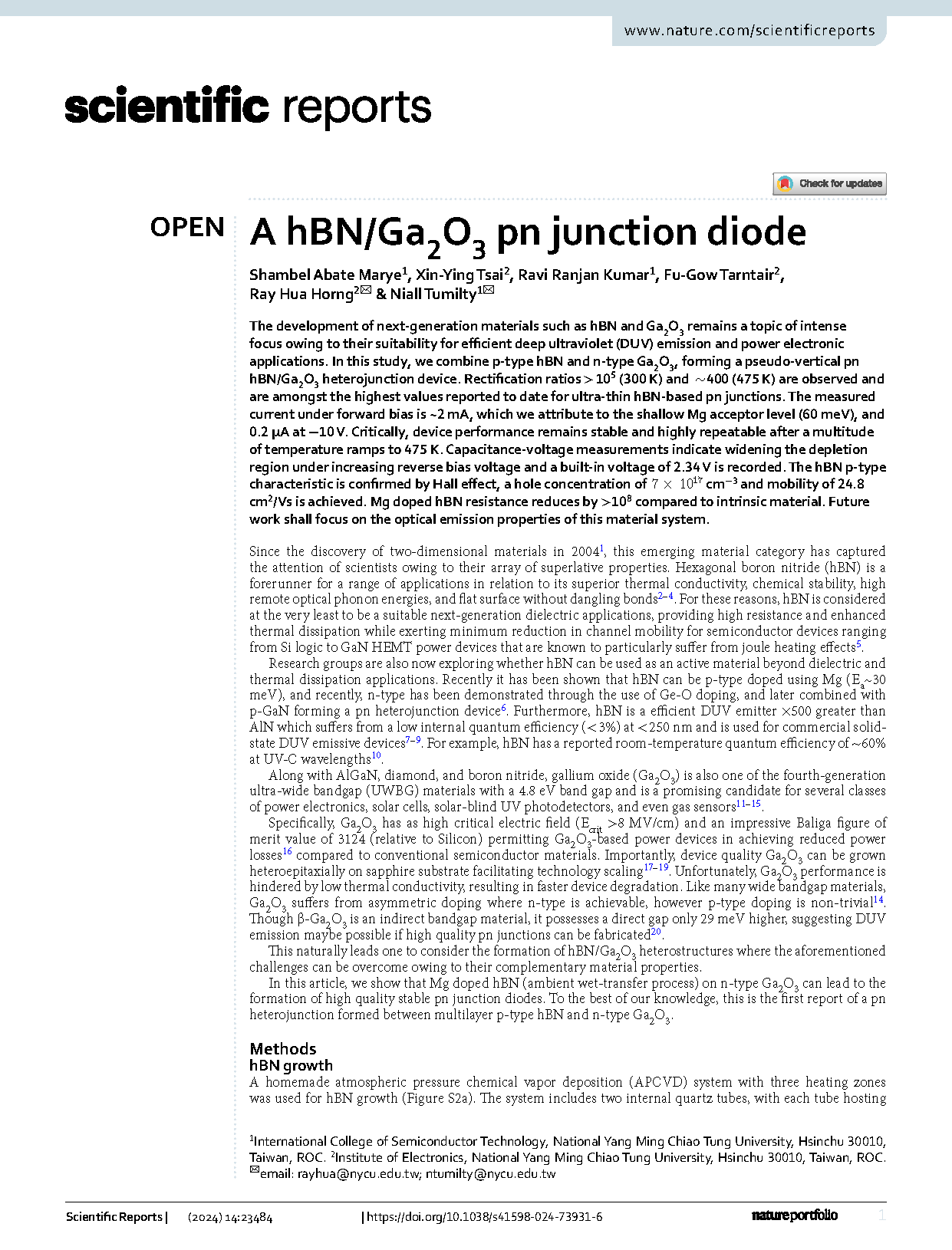
Fig. 1 (a) pn junction diode fabrication process, (b) schematic of device structure and (c) the optical microscope (OM) image of the fabricated device (the scale bar is 400 μm).
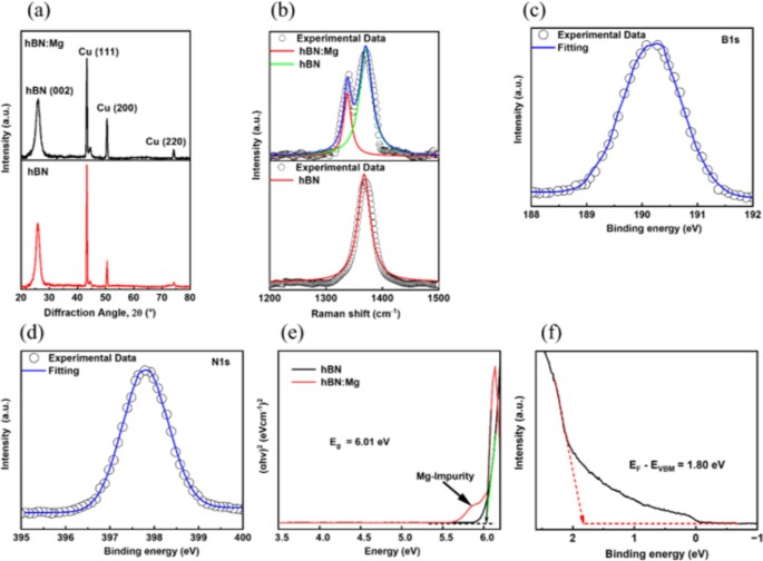
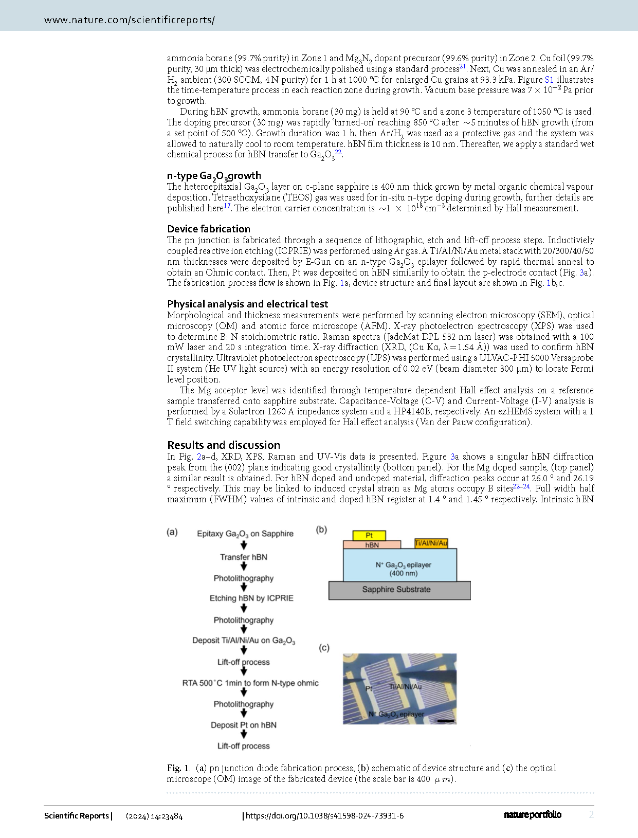
Fig. 2 (a) XRD spectrum of hBN (b) Raman spectrum (c, d) XPS spectra of B1s and N1s of Mg doped hBN (e) UV-VIS Tauc plot (f) UPS analysis of Mg doped hBN.
DOI:
doi.org/10.1038/s41598-024-73931-6