Paper Sharing
【Member Papers】Researchers from the Shanghai Institute of Microsystem and Information Technology, Chinese Academy of Sciences, investigated the extremely low thermal resistance of β-Ga₂O₃ MOSFETs achieved through the co-integrated design of substrate engineering and device packaging.
日期:2024-12-06阅读:972
Researchers from the Shanghai Institute of Microsystem and Information Technology, Chinese Academy of Sciences have published a dissertation titled "Extremely Low Thermal Resistance of β-Ga2O3 MOSFETs by Co-integrated Design of Substrate Engineering and Device Packaging" in ACS Applied Materials & Interfaces.
Abstract
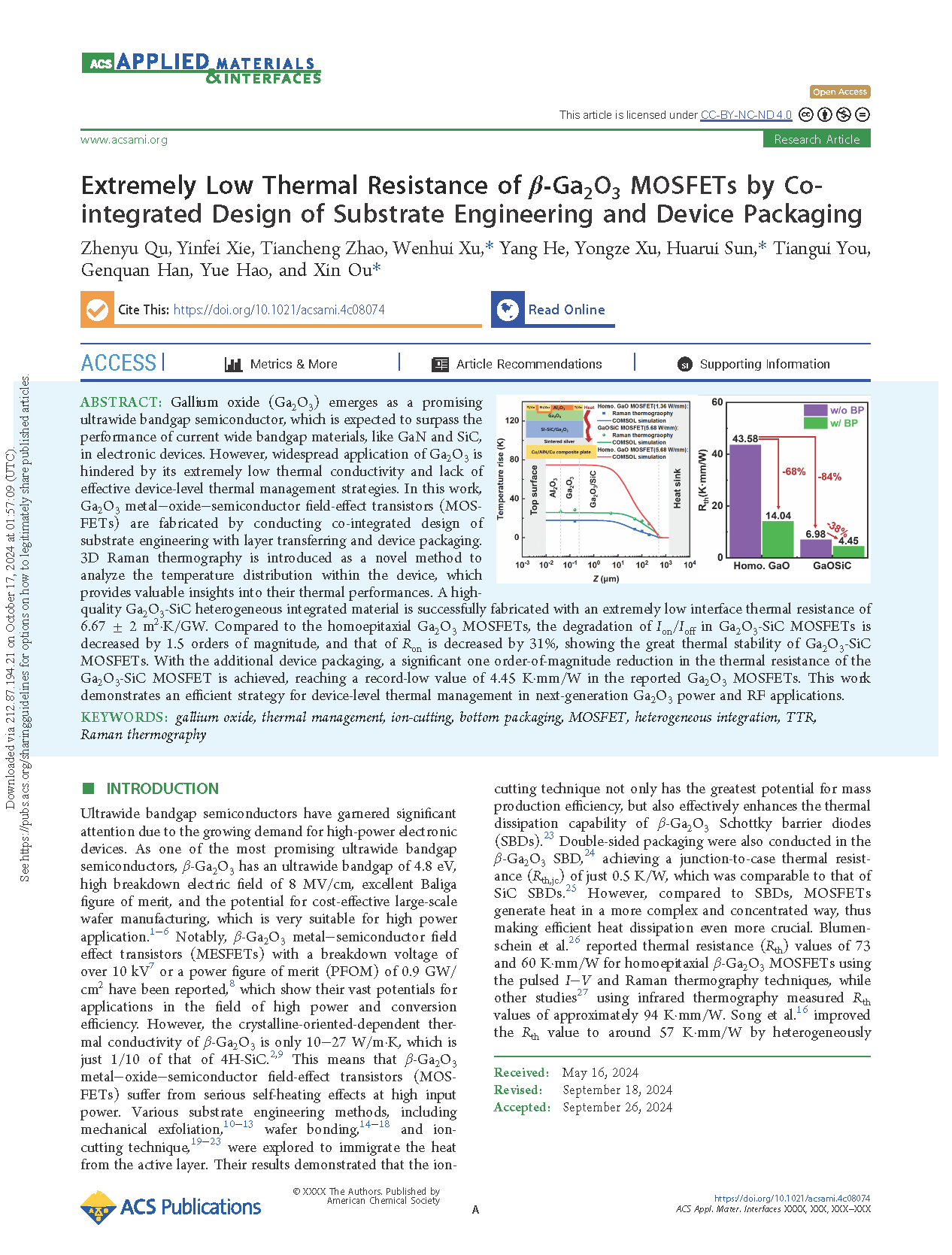
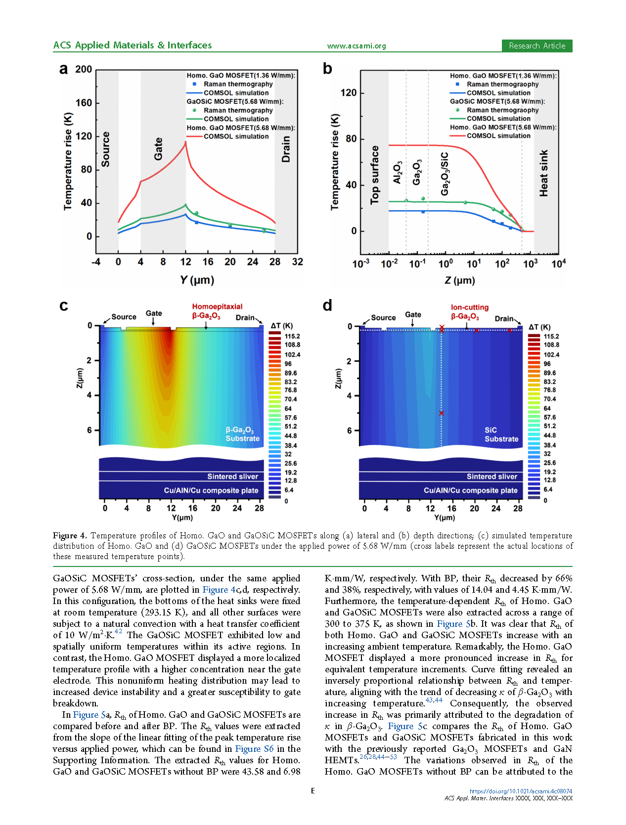
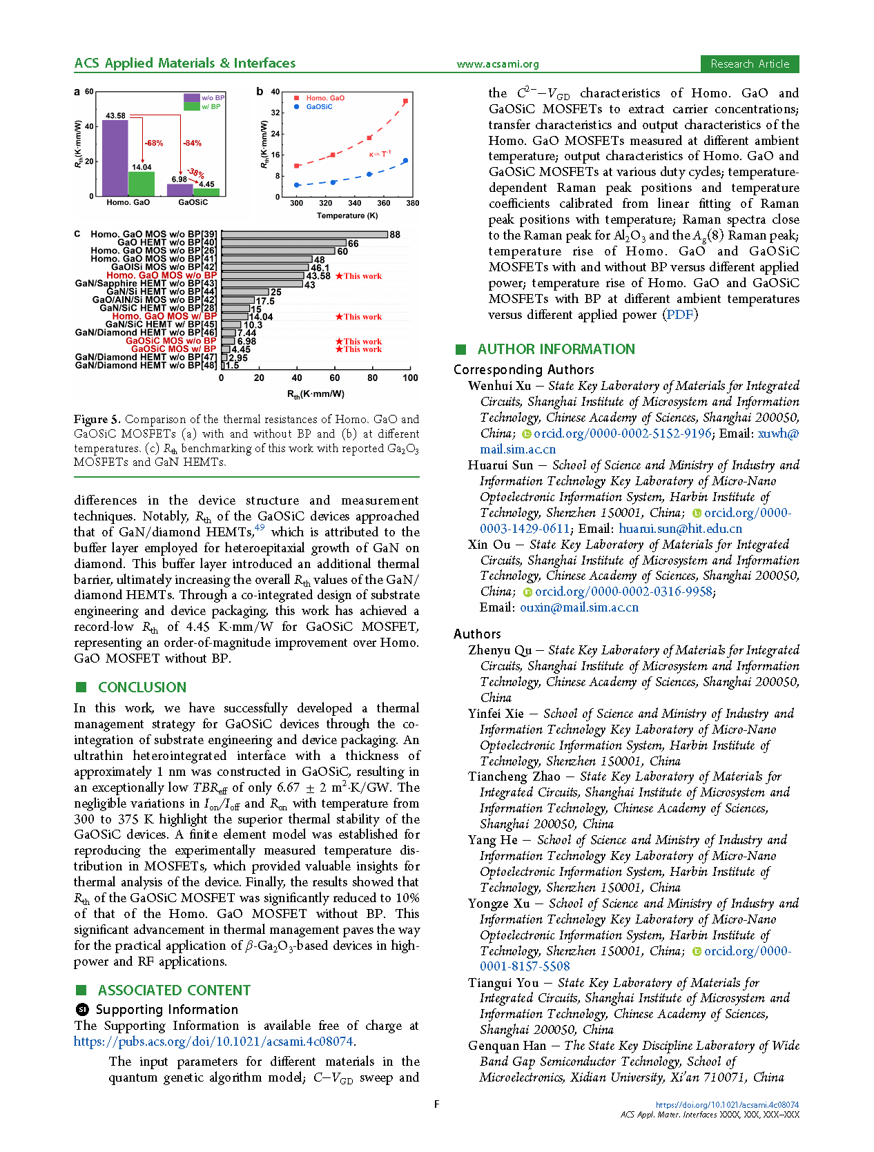
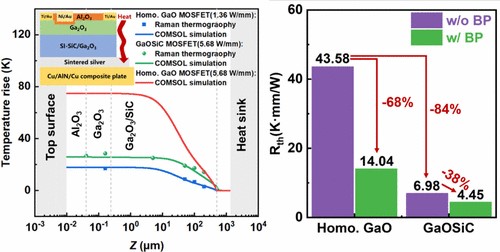
Gallium oxide (Ga2O3) emerges as a promising ultrawide bandgap semiconductor, which is expected to surpass the performance of current wide bandgap materials, like GaN and SiC, in electronic devices. However, widespread application of Ga2O3 is hindered by its extremely low thermal conductivity and lack of effective device-level thermal management strategies. In this work, Ga2O3 metal–oxide–semiconductor field-effect transistors (MOSFETs) are fabricated by conducting co-integrated design of substrate engineering with layer transferring and device packaging. 3D Raman thermography is introduced as a novel method to analyze the temperature distribution within the device, which provides valuable insights into their thermal performances. A high-quality Ga2O3-SiC heterogeneous integrated material is successfully fabricated with an extremely low interface thermal resistance of 6.67 ± 2 m2·K/GW. Compared to the homoepitaxial Ga2O3 MOSFETs, the degradation of Ion/Ioff in Ga2O3-SiC MOSFETs is decreased by 1.5 orders of magnitude, and that of Ron is decreased by 31%, showing the great thermal stability of Ga2O3-SiC MOSFETs. With the additional device packaging, a significant one order-of-magnitude reduction in the thermal resistance of the Ga2O3-SiC MOSFET is achieved, reaching a record-low value of 4.45 K·mm/W in the reported Ga2O3 MOSFETs. This work demonstrates an efficient strategy for device-level thermal management in next-generation Ga2O3 power and RF applications.
DOI:
https://doi.org/10.1021/acsami.4c08074