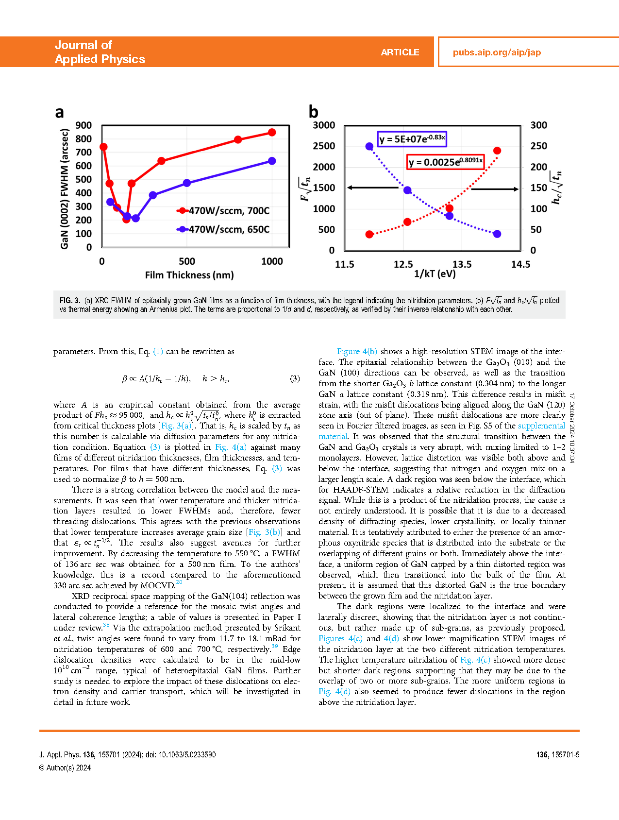
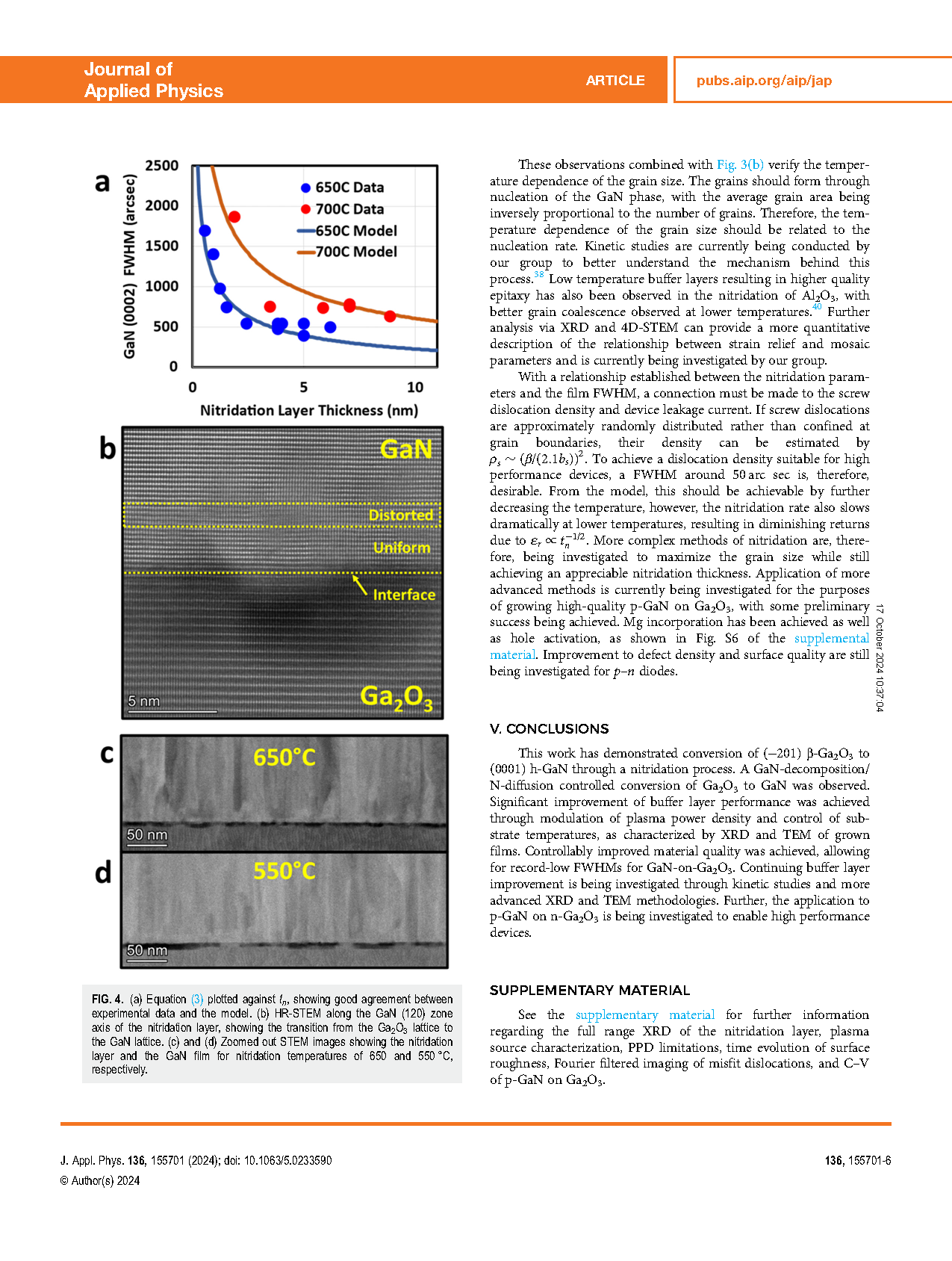
Paper Sharing
【International Papers】Epitaxial growth of GaN on β-Ga₂O₃ via RF plasma nitridation
日期:2024-12-11阅读:876
Researchers from the University of Illinois at Urbana-Champaign have published a dissertation titled "Epitaxial growth of GaN on β-Ga2O3 via RF plasma nitridation" in Journal of Applied Physics.
Abstract
The lack of suitable p-type dopant for β-Ga2O3 remains a hurdle for vertical power device applications. Epitaxy of GaN on Ga2O3 substrates was demonstrated as an alternative. (–201)-oriented β-Ga2O3 was converted into (0001)-oriented hexagonal GaN via nitrogen plasma in a plasma-assisted molecular beam epitaxy chamber, as verified by XRD and RHEED. The resulting nitridated GaN layers were characterized by TEM, x-ray reflectivity, and AFM to relate the nitridation conditions to crystallinity, layer thickness, and surface roughness. The crystallinity of subsequently grown epitaxial GaN films was quantified via XRD rocking curves and related to the nitridation layer properties across varying nitridation conditions. Specifically, the effect of the grain size and nitridation layer thickness was investigated to determine their role in threading screw dislocation management.
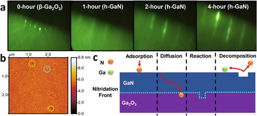
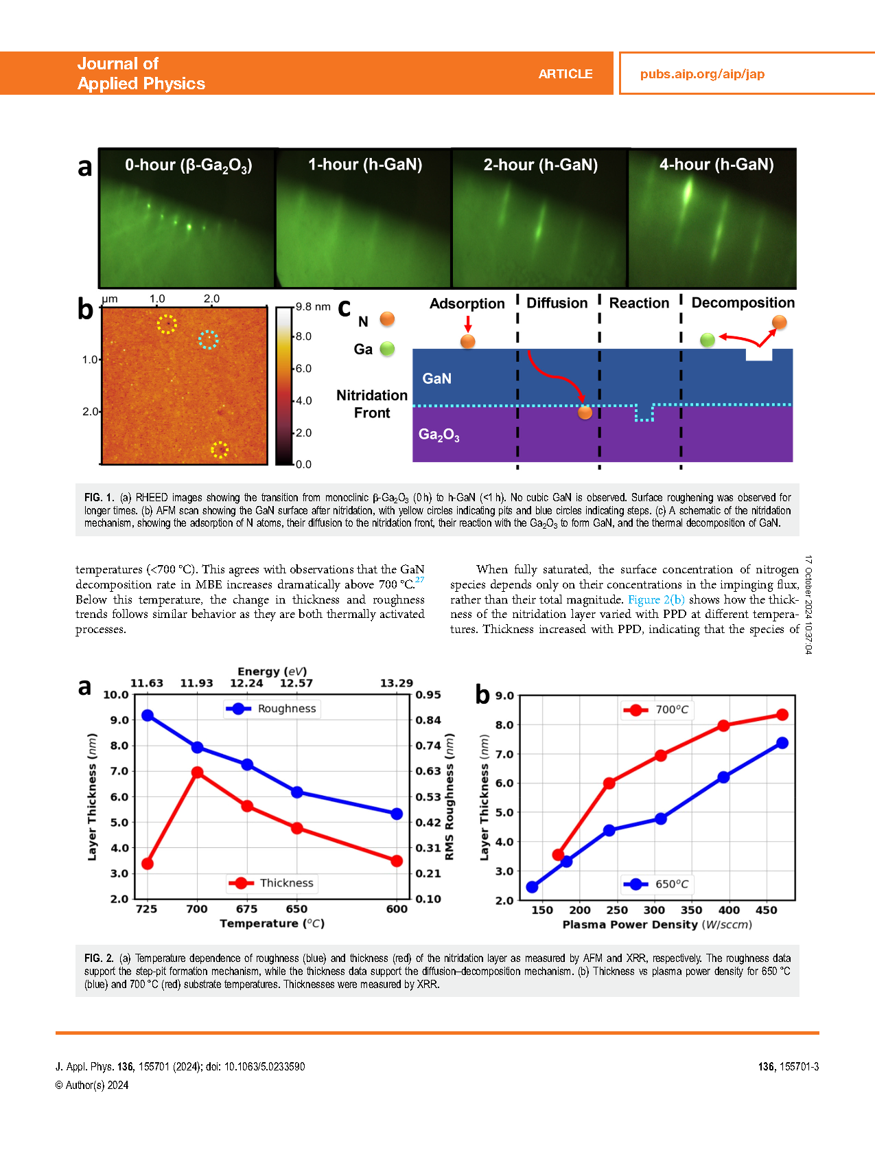
FIG. 1. (a) RHEED images showing the transition from monoclinic β-Ga2O3 (0 h) to h-GaN (<1 h). No cubic GaN is observed. Surface roughening was observed for longer times. (b) AFM scan showing the GaN surface after nitridation, with yellow circles indicating pits and blue circles indicating steps. (c) A schematic of the nitridation mechanism, showing the adsorption of N atoms, their diffusion to the nitridation front, their reaction with the Ga2O3 to form GaN, and the thermal decomposition of GaN.
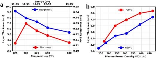
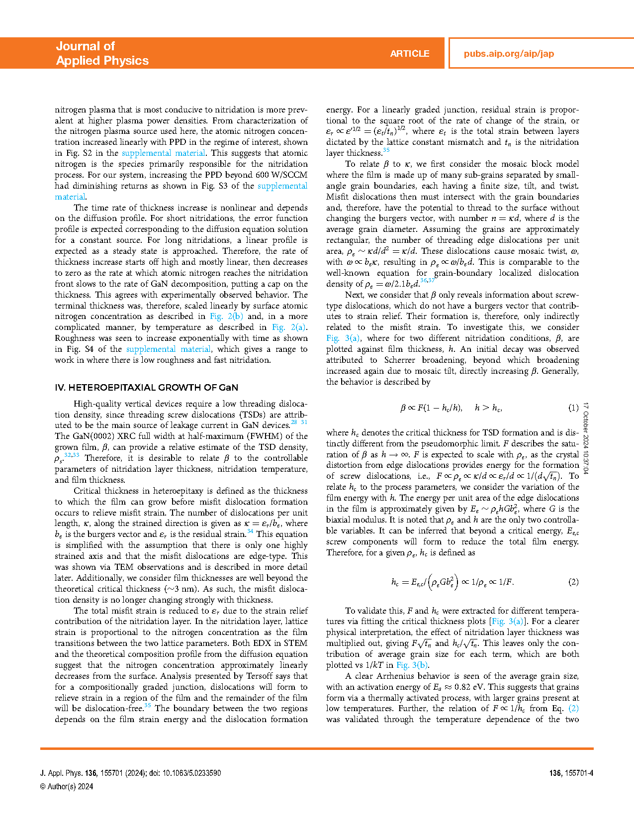
FIG. 2. (a) Temperature dependence of roughness (blue) and thickness (red) of the nitridation layer as measured by AFM and XRR, respectively. The roughness data support the step-pit formation mechanism, while the thickness data support the diffusion–decomposition mechanism. (b) Thickness vs plasma power density for 650 °C (blue) and 700 °C (red) substrate temperatures. Thicknesses were measured by XRR.
DOI:
doi.org/10.1063/5.0233590