
【International Papers】Epilayer thickness effect on the electrical and breakdown characteristics of vertical β-Ga₂O₃ Schottky barrier diode
日期:2024-12-17阅读:807
Researchers from the Jeonbuk National University have published a dissertation titled "Epilayer thickness effect on the electrical and breakdown characteristics of vertical β-Ga2O3 Schottky barrier diode" in Journal of Crystal Growth.
Abstract
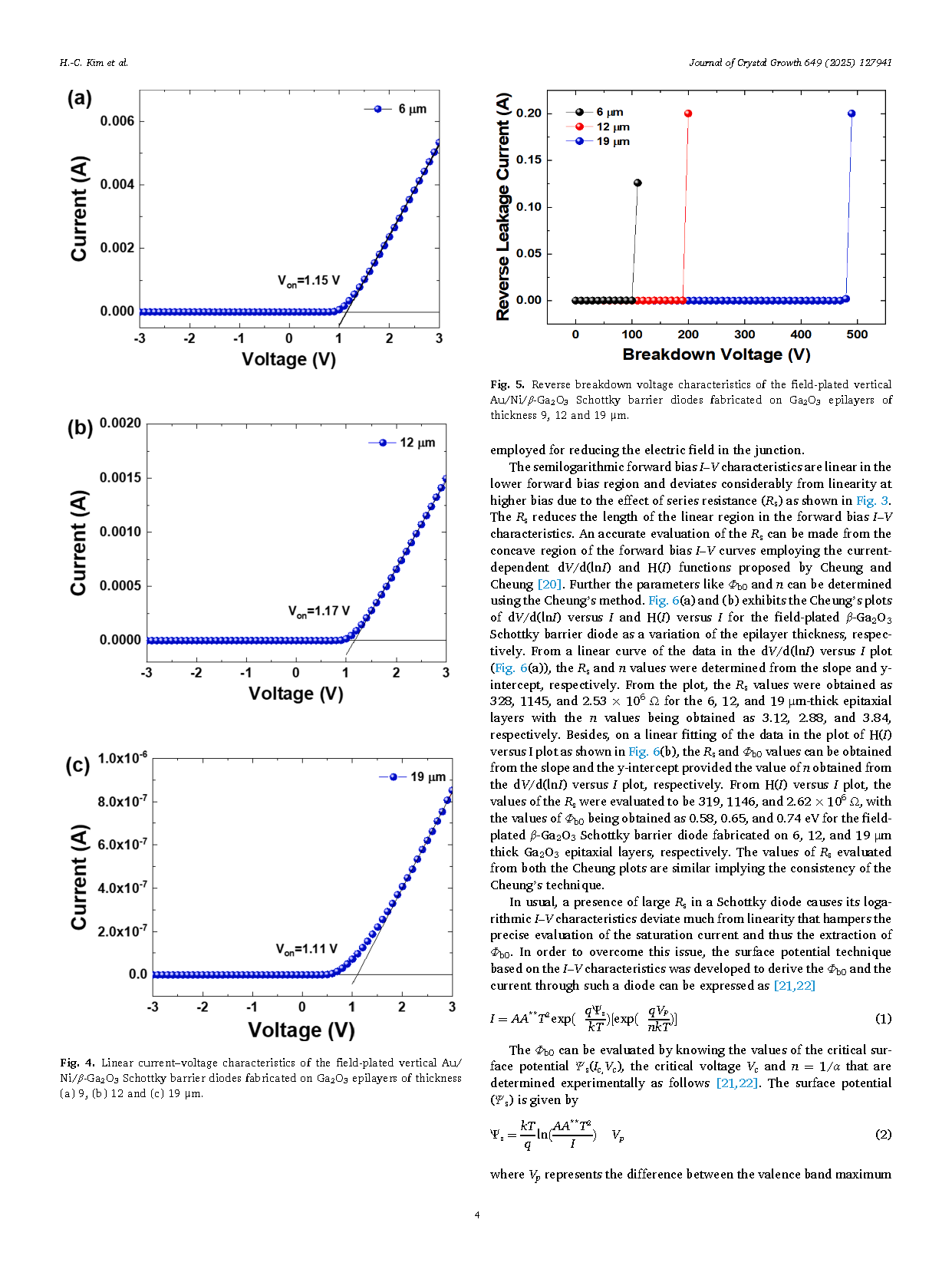
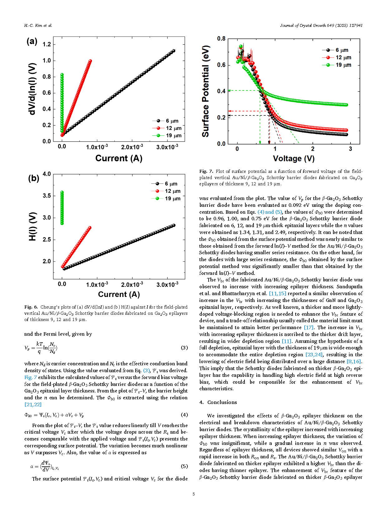
The current–voltage and breakdown characteristics of Au/Ni/β-Ga2O3 Schottky barrier diodes were investigated as a function of β-Ga2O3 epilayer thickness in the range of 6–19 μm. The X-ray rocking curves indicated that the full-width half-maximum is reduced with increasing epilayer thickness, implying an improvement in the crystallinity of β-Ga2O3 epilayer. The barrier heights of the field-plated β-Ga2O3 Schottky barrier diode with epitaxial layer thickness of 6, 12, and 19 μm were obtained as 1.01, 1.03, and 1.04 eV, with the ideality factor values being 1.21, 1.19, and 1.46, respectively. The higher ideality factors could be associated with the existence of inhomogeneity at the metal–semiconductor interface. The series resistance of the Schottky diode obtained increased with increasing epilayer thickness. The Schottky diode fabricated on 19 μm thick epitaxial layer exhibited a higher breakdown voltage of 490 V. The increase in epilayer thickness led to the widening of depletion region, resulting in lower electric field over a larger distance. This could be a main cause of the enhancement of the breakdown voltage characteristics of β-Ga2O3 Schottky barrier diode.
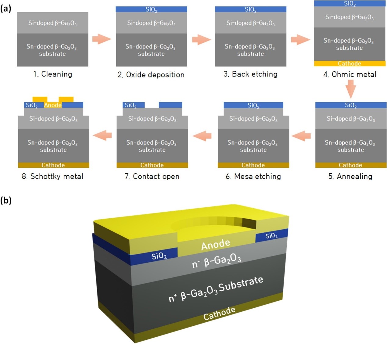
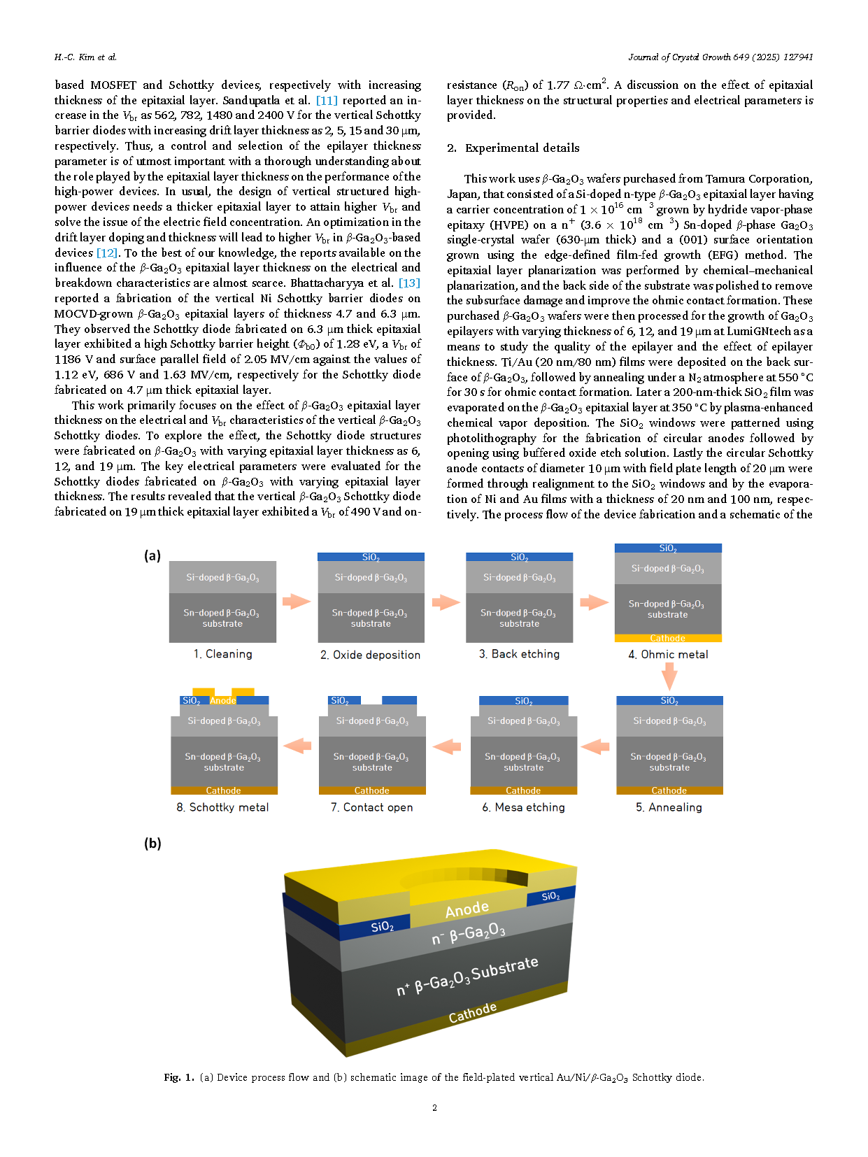
Fig. 1. (a) Device process flow and (b) schematic image of the field-plated vertical Au/Ni/β-Ga2O3 Schottky diode.
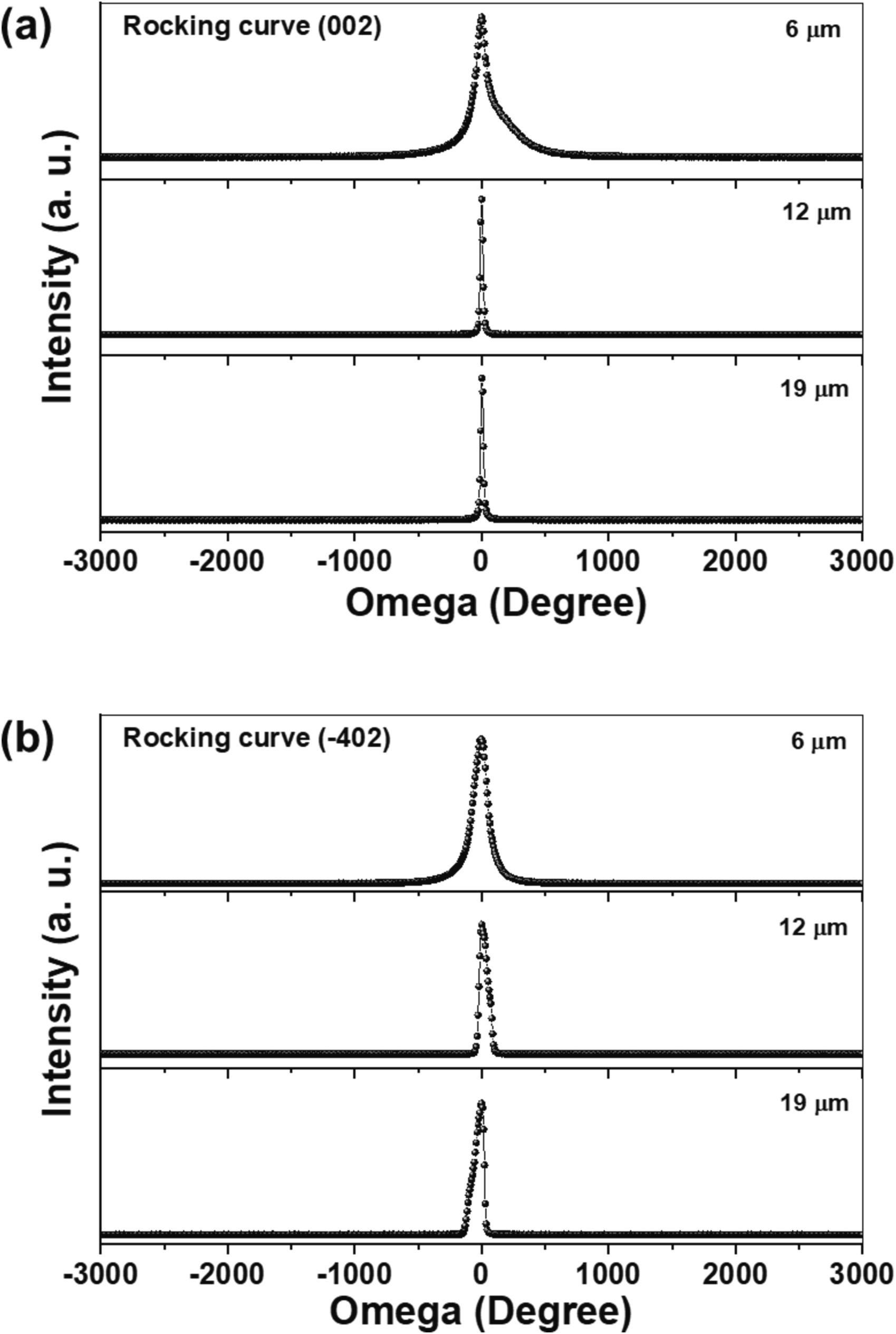
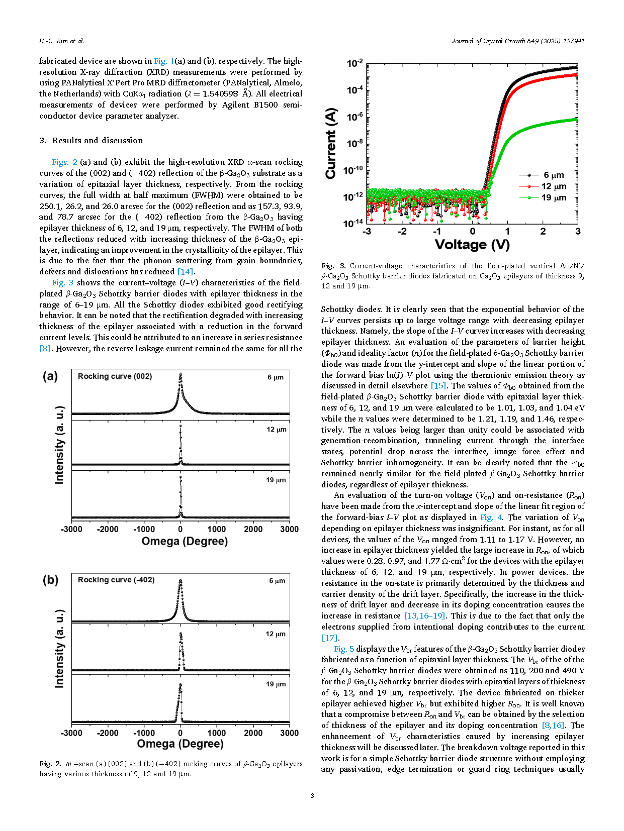
Fig. 2. ω −scan (a) (002) and (b) (−402) rocking curves of β-Ga2O3 epilayers having various thickness of 9, 12 and 19 μm.
DOI:
doi.org/10.1016/j.jcrysgro.2024.127941

