
【Member Papers】Northeast Normal University ——Dressing AgNWs with MXenes Nanosheets: Transparent Printed Electrodes Combining High-Conductivity and Tunable Work Function for High-Performance Opto-Electronics
日期:2024-12-17阅读:793
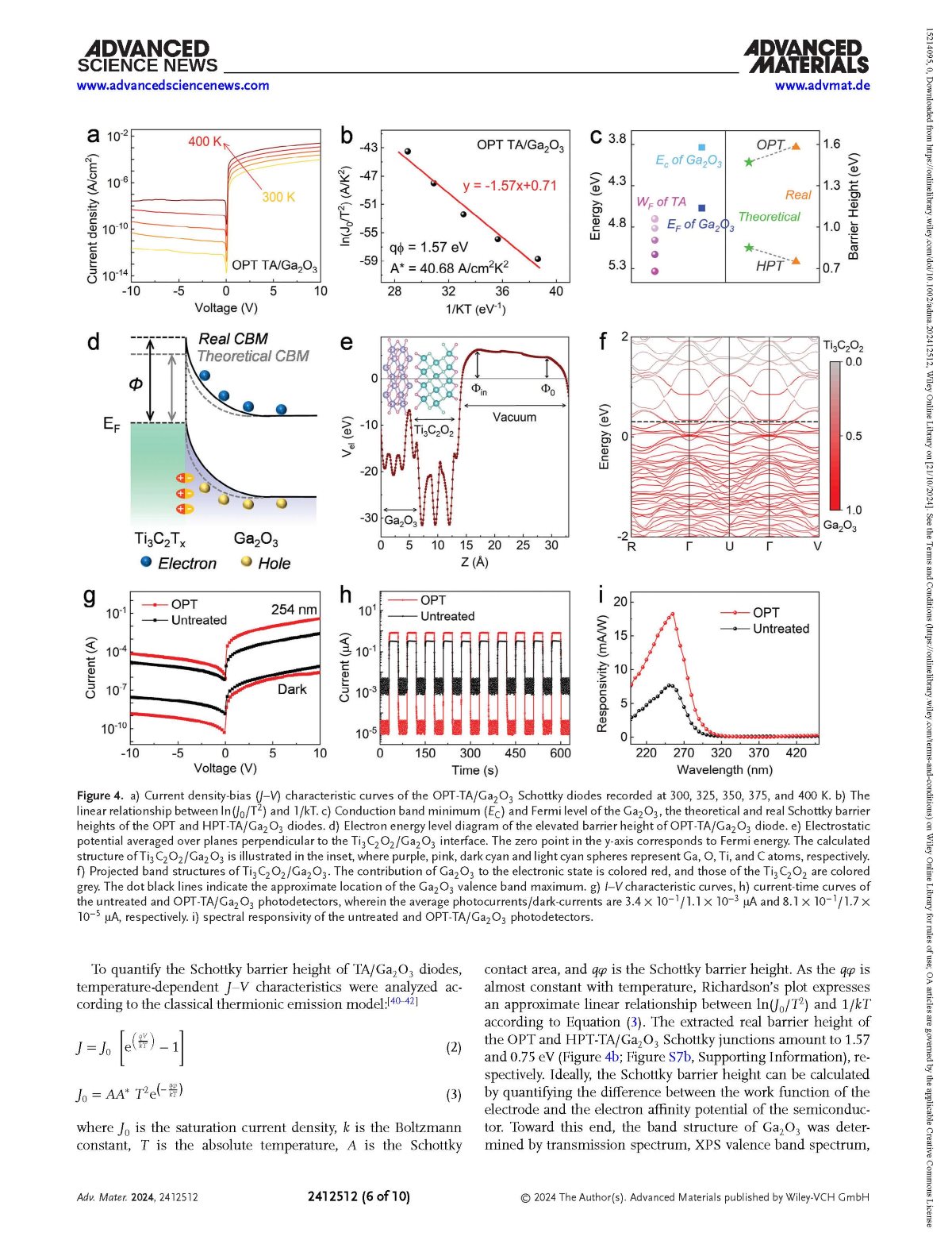
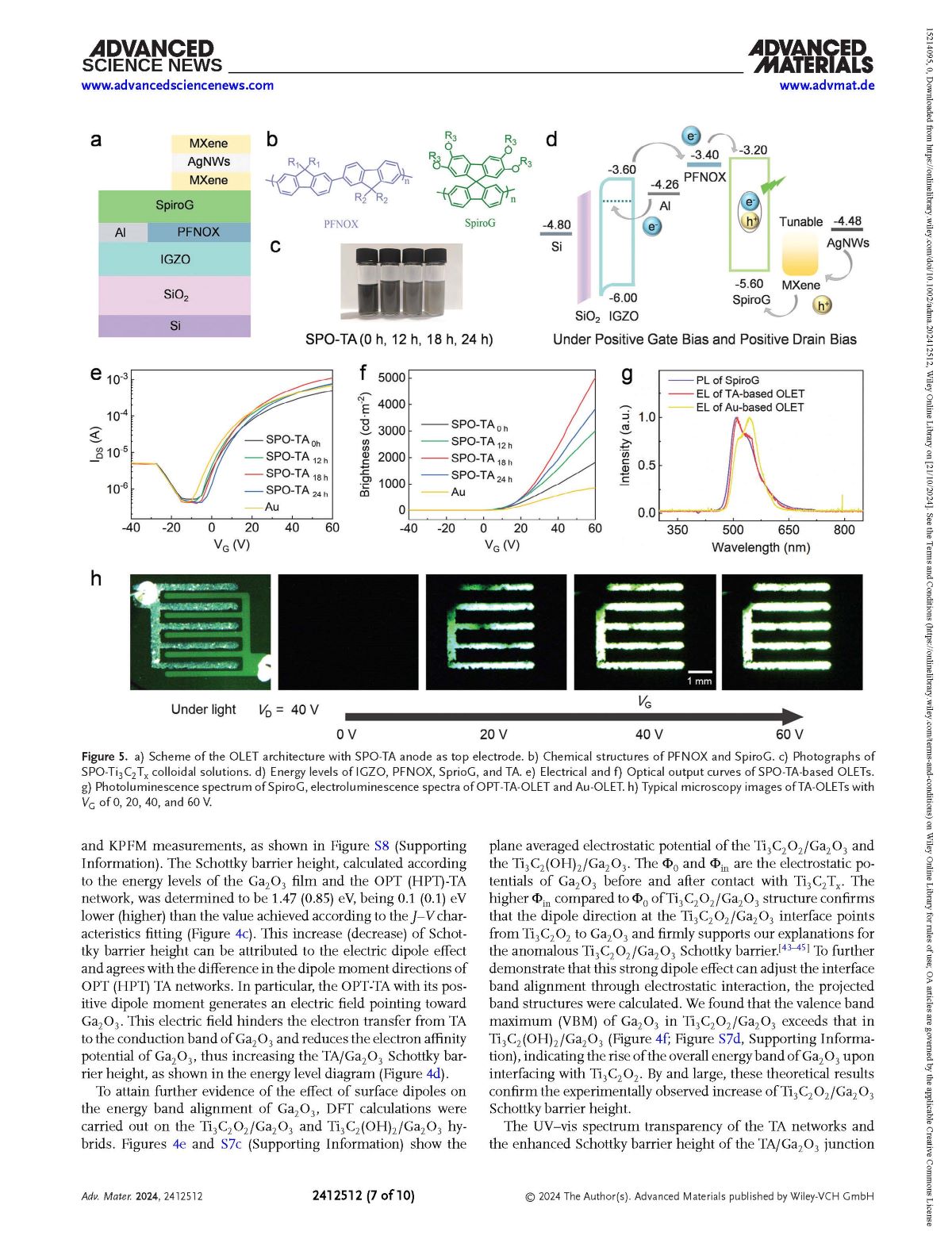
Researchers from the Northeast Normal University have published a dissertation titled "Dressing AgNWs with MXenes Nanosheets: Transparent Printed Electrodes Combining High-Conductivity and Tunable Work Function for High-Performance Opto-Electronics" in Advanced Materials.
Abstract
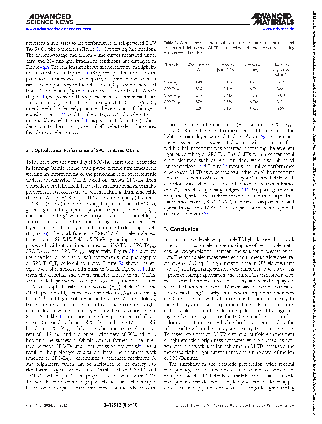
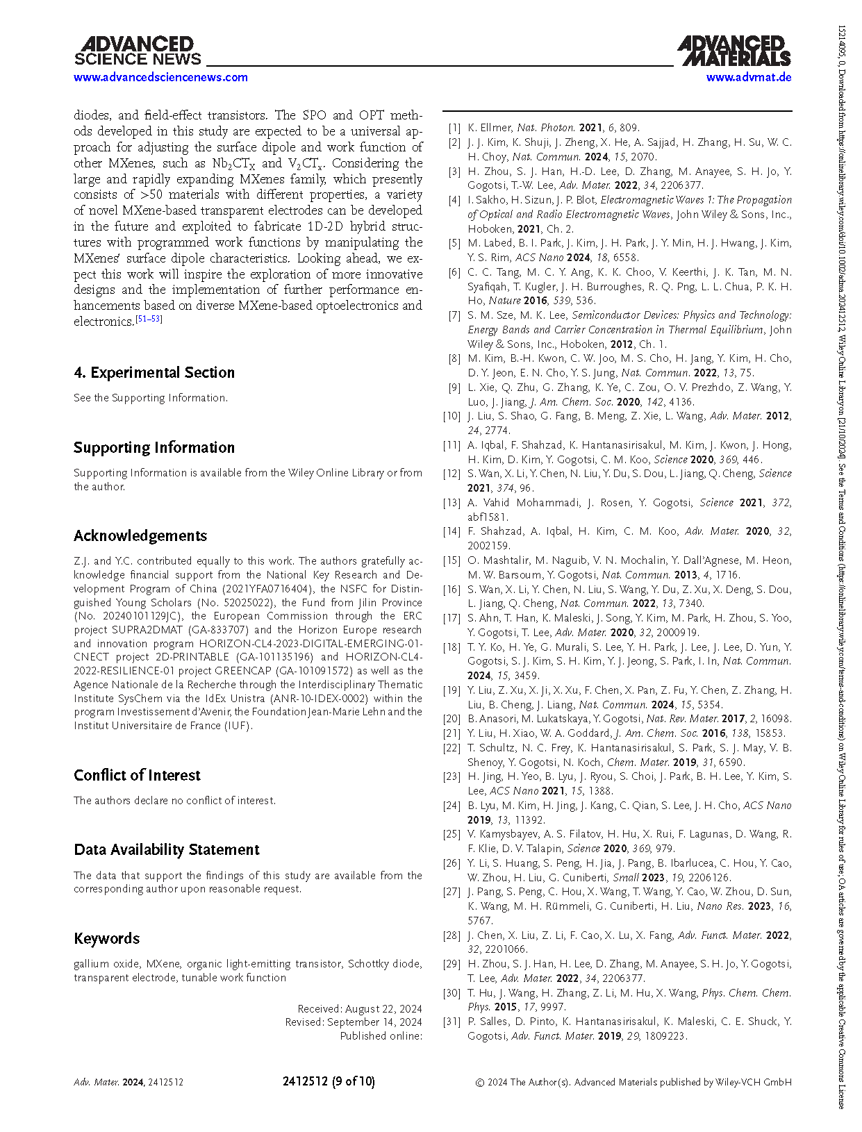
High-work function transparent electrodes (HWFTEs) are key for establishing Schottky and Ohmic contacts with n-type and p-type semiconductors, respectively. However, the development of printable materials that combine high transmittance, low sheet resistance, and tunable work function remains an outstanding challenge. This work reports a high-performance HWFTE composed of Ag nanowires enveloped conformally by Ti3C2Tx nanosheets (TA), forming a shell-core network structure. The printed TA HWFTEs display an ultrahigh transmittance (>94%) from the deep-ultraviolet (DUV) to the entire visible spectral region, a low sheet resistance (<15 Ω sq−1), and a tunable work function ranging from 4.7 to 6.0 eV. The introduction of additional oxygen terminations on the Ti3C2Tx surface generates positive dipoles, which not only increases the work function of the TA HWFTEs but also elevates the TA/Ga2O3 Schottky barrier, resulting in a high self-powered responsivity of 18 mA W−1 in Ga2O3 diode DUV photodetectors, as demonstrated via experimental characterizations and theoretical calculations. Furthermore, the TA HWFTEs-based organic light-emitting transistors exhibit exceptional emission brightness of 5020 cd m−2, being four-fold greater than that in Au electrodes-based devices. The innovative nano-structure design, work function tuning, and the revealed mechanisms of electrode-semiconductor contact physics constitute a substantial advancement in high-performance optoelectronic technology.
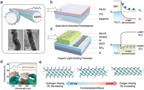
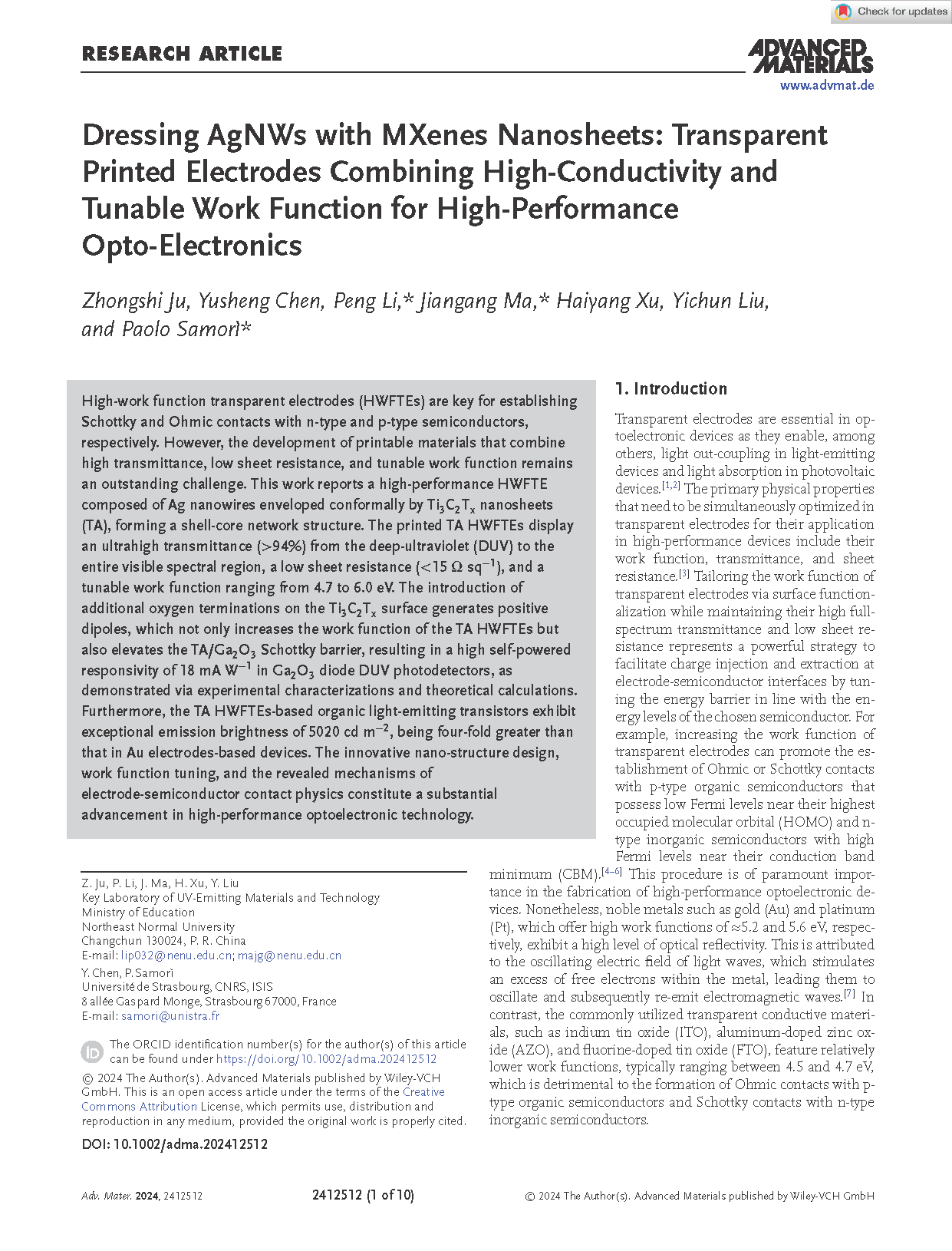
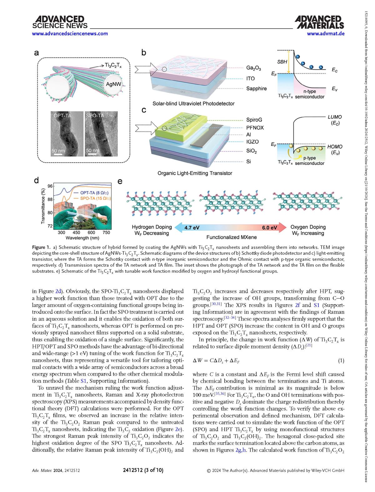
Figure 1. a) Schematic structure of hybrid formed by coating the AgNWs with Ti3C2Tx nanosheets and assembling them into networks. TEM image depicting the core-shell structure of AgNWs-Ti3C2Tx. Schematic diagrams of the device structures of b) Schottky diode photodetector and c) light-emitting transistor, where the TA forms the Schottky contact with n-type inorganic semiconductor and the Ohmic contact with p-type organic semiconductor, respectively. d) Transmission spectra of the TA network and TA film. The inset shows the photograph of the TA network and the TA film on the flexible substrates. e) Schematic of the Ti3C2Tx with tunable work function modified by oxygen and hydroxyl functional groups.
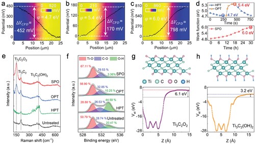
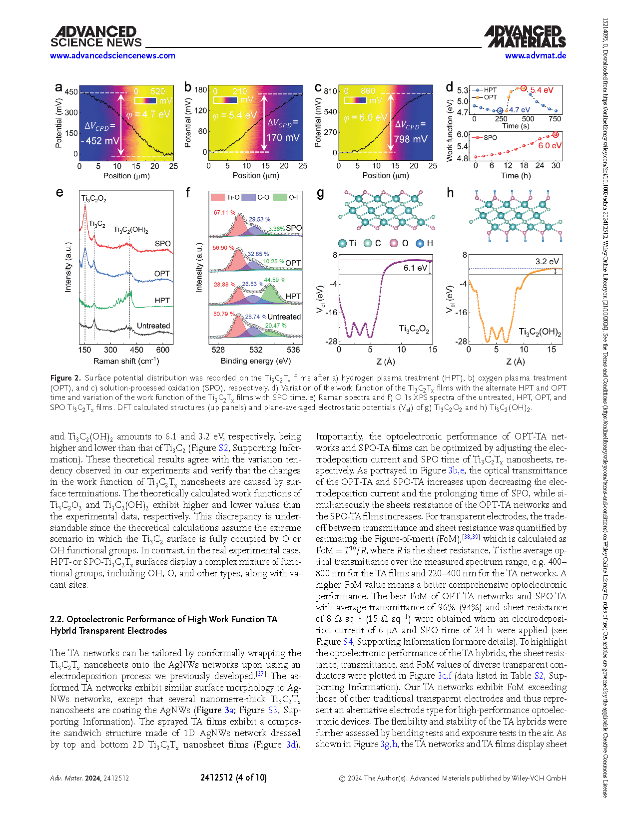
Figure 2. Surface potential distribution was recorded on the Ti3C2Tx films after a) hydrogen plasma treatment (HPT), b) oxygen plasma treatment (OPT), and c) solution-processed oxidation (SPO), respectively. d) Variation of the work function of the Ti3C2Tx films with the alternate HPT and OPT time and variation of the work function of the Ti3C2Tx films with SPO time. e) Raman spectra and f) O 1s XPS spectra of the untreated, HPT, OPT, and SPO Ti3C2Tx films. DFT calculated structures (up panels) and plane-averaged electrostatic potentials (Vel) of g) Ti3C2O2 and h) Ti3C2(OH)2.
DOI:
doi.org/10.1002/adma.202412512
