
【Substrate Papers】Research on Positron Annihilation Spectroscopy of Defect and Electrical Conductivity in Sn-Doped β-Ga₂O₃ Semiconductors
日期:2024-12-31阅读:866
Chip is the "crown" in the field of science and technology, and the performance parameters of the semiconductor directly determine the performance of the chip. Since 2020, the United States has successively issued more than a dozen sanctions on China's semiconductor industry chain, and China has correspondingly carried out export controls on semiconductor materials to the United States.
As a new fourth-generation semiconductor material, β-Ga2O3 has many excellent properties, such as ultra-wide bandgap (4.5-4.9eV), large breakdown voltage, high temperature resistance and radiation resistance, showing great application prospects. In order to improve the N-type conductive properties of β-Ga2O3, the carrier concentration of β-Ga2O3 is mainly increased by doping Si, Ge, Sn and other element. However, in most experiments, the carrier concentration of β-Ga2O3 is smaller than the doping concentration, which indicates that there are defect in β-Ga2O3 that affect the electrical conductivity. In order to develop the performance of β-Ga2O3 semiconductor devices, it is important to deeply study the influence of defect and macroscopic conductivity properties. The annihilation process of positron in semiconductor is highly sensitive to the crystal structure, defect distribution, momentum distribution and electron density distribution, and the positron annihilation experiment can provide a strong evidence for the defect structure analysis of β-Ga2O3 materials.
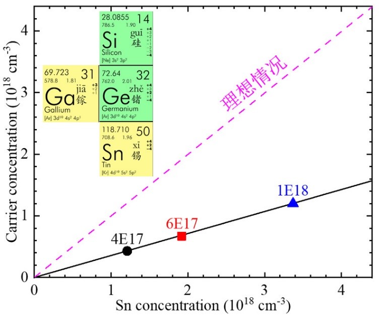
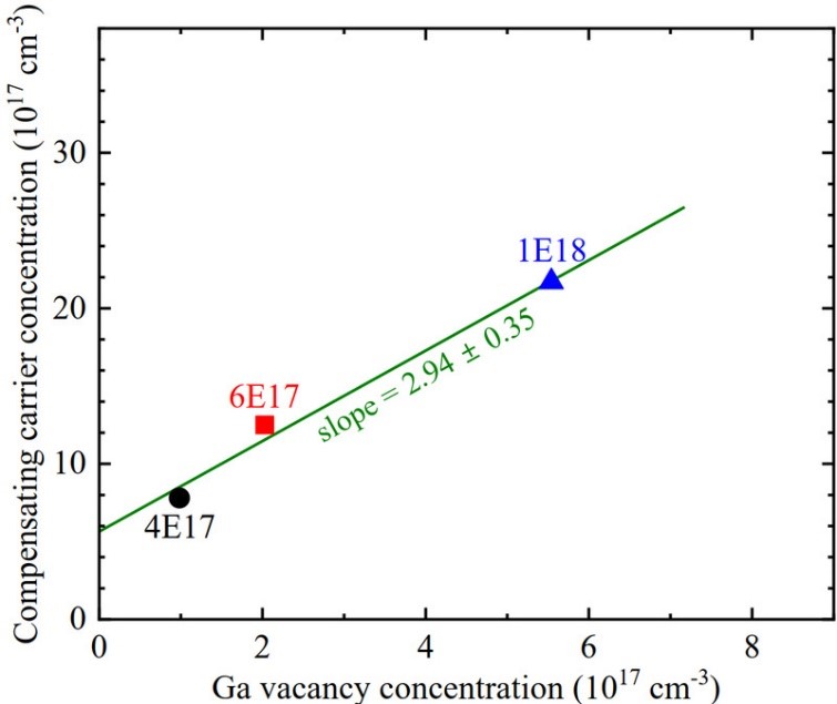
With the support of the National key R&D Program "Nanotechnology" key project "Research on Momentum Space Spectroscopy of Nanostructures and New Multi-Parameter Positron Spectroscopy Characterization of Nanothin Films", Particle Beam Cross Application Laboratory of the University of Science and Technology of China studied three different Sn doped β-Ga2O3 crystals prepared by EFG method using positron annihilation spectroscopy. As shown in Figure 1(a), Sn has one more outermost electron than Ga, and ideally the carrier concentration provided should be comparable to the Sn doping concentration. However, in practice, the carrier concentration is about one-third of the Sn doping concentration, which indicates that there is a defect in the sample to compensate for the carrier concentration. Positron annihilation lifetime experiments and theoretical calculations show that the lifetime of 175-190 ps measured in all positron annihilation studies of β-Ga2O3 is the lifetime of Ga vacancy, not the bulk lifetime of β- Ga2O3. The positron annihilation lifetime derived vacancy concentrations indicate the presence of high concentrations of Ga vacancies in all three samples. As shown in Figure 1(b), the relationship between compensated carrier concentration (Sn doping concentration minus Ga vacancy concentration) and Ga vacancy concentration indicates that these vacancies are -3 valence and are major receptor defect.


Figure 1. (a) the relationship between the carrier concentration and the Sn doping concentration, and (b) the relationship between the compensated carrier concentration and the Ga vacancy concentration.
The work has been published on November 7, 2024 in Physical Review B, a well-known journal in the field of Physics of Condensed Matter. Titled "Ga vacancies as dominant intrinsic acceptors in Sn-doped beta -Ga2O3 revealed by positron annihilation spectroscopy" (Phys. Rev. B 110, 174106 (2024)). The first author of the paper is Yuhuan Li, a PhD student in the Particle Beam Cross Application Laboratory and corresponding authors are Guangwei Xu Special Research Fellow (College of Microelectronics of USTC) and Hongjun Zhang Special Research Fellow.


