
【International Papers】Proton irradiation Of Ga₂O₃ Schottky diodes and NiO/Ga₂O₃ heterojunctions
日期:2024-12-31阅读:832
Researchers from the National University of Science and Technology MISIS have published a dissertation titled "Proton irradiation Of Ga2O3 Schottky diodes and NiO/Ga2O3 heterojunctions" in Scientific Reports.
Abstract
p-NiO/n-Ga2O3 heterojunction (HJ) diodes exhibit much larger changes in their properties upon 1.1 MeV proton irradiation than Schottky diodes (SDs) prepared on the same material. In p-NiO/Ga2O3 HJ diodes, the narrow region adjacent to the HJ boundary is found to contain a high density of relatively deep centers with levels near EC-0.17 eV and a depleted region in the immediate vicinity of the HJ boundary. The series resistance of the HJ diodes is slightly higher than for the Schottky diodes and shows a temperature dependence with activation energy ~ 0.12 eV, like the temperature dependence of the NiO film resistivity. Irradiation with 1.1 MeV protons leads to a decrease of the hole concentration in the NiO, with a high carrier removal rate of ~ 1.3 × 105 cm−1 and a strong compensation of the interfacial region where the concentration of the EC-0.17 eV centers decreases with a high rate of ~ 7 × 103 cm−1. The combined action of these two effects gives rise to the much stronger increase of the series resistance of the HJ diodes compared to Schottky diodes. The observed differences between the radiation response of the HJs and SDs cannot be credibly attributed to the changes of the density of any of the deep electron and hole traps detected in our experiments.
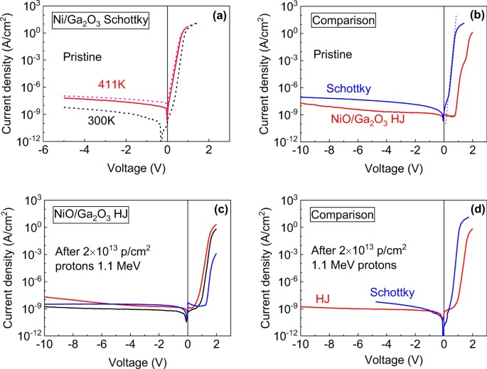
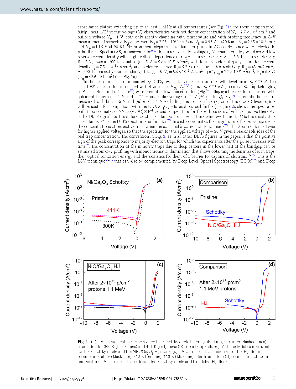
Fig. 1 (a) J-V characteristics measured for the Schottky diode before (solid lines) and after (dashed lines) irradiation for 300 K (black lines) and 411 K (red) lines; (b) room temperature J-V characteristics measured for the Schottky diode and the NiO/Ga2O3 HJ diode; (c) J-V characteristics measured for the HJ diode at room temperature (black line), 412 K (red line), 113 K (blue line) after irradiation; (d) comparison of room temperature J-V characteristics of irradiated Schottky diode and irradiated HJ diode.
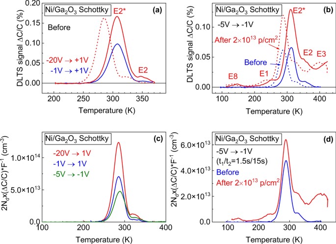
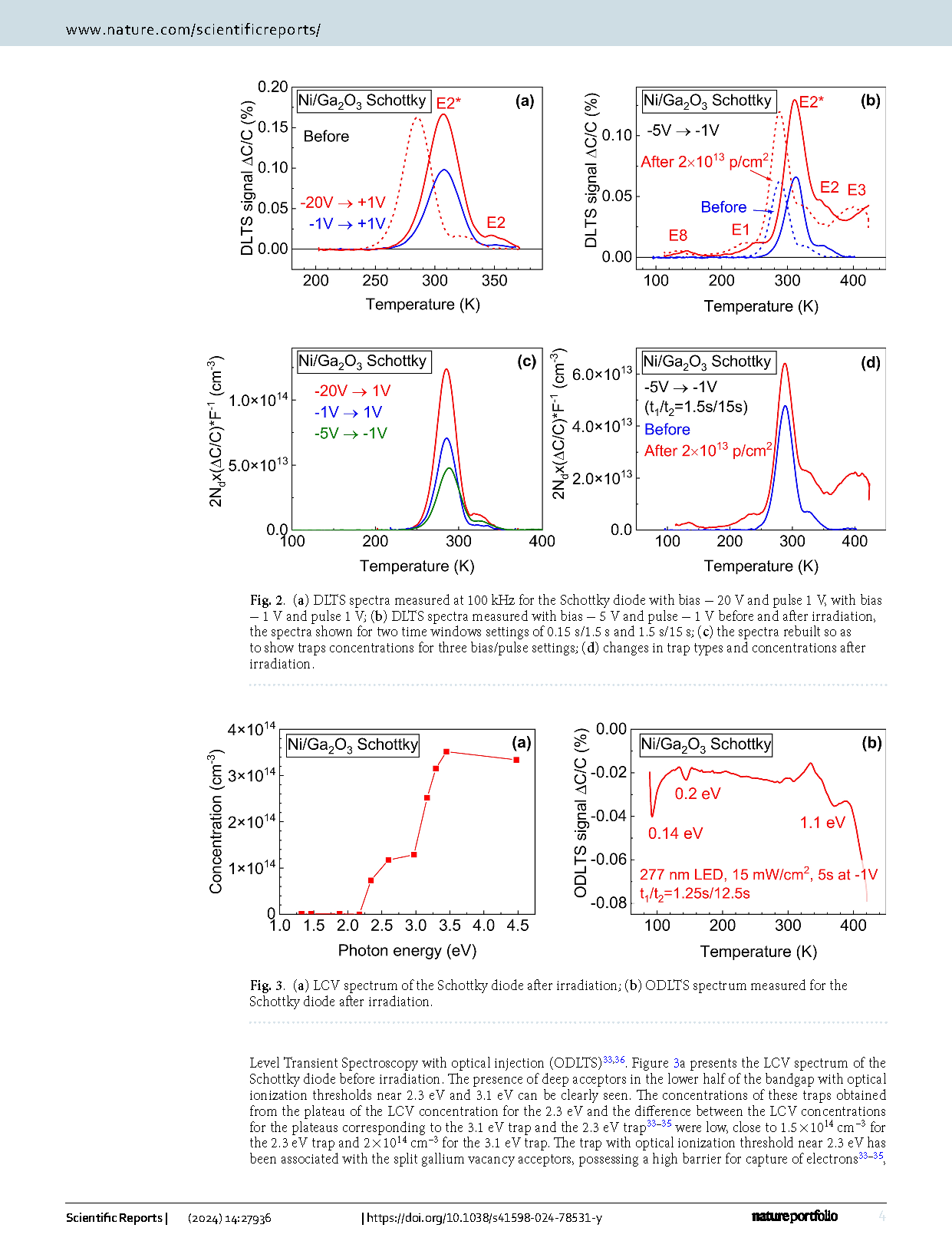
Fig. 2 (a) DLTS spectra measured at 100 kHz for the Schottky diode with bias − 20 V and pulse 1 V, with bias − 1 V and pulse 1 V; (b) DLTS spectra measured with bias − 5 V and pulse − 1 V before and after irradiation, the spectra shown for two time windows settings of 0.15 s/1.5 s and 1.5 s/15 s; (c) the spectra rebuilt so as to show traps concentrations for three bias/pulse settings; (d) changes in trap types and concentrations after irradiation.
DOI:
doi.org/10.1038/s41598-024-78531-y
