
【Domestic Papers】Retina-Inspired X-Ray Optoelectronic Synapse Using Amorphous Ga₂O₃ Thin Film
日期:2024-12-31阅读:802
Researchers from the Songshan Lake Materials Laboratory have published a dissertation titled "Retina-Inspired X-Ray Optoelectronic Synapse Using Amorphous Ga2O3 Thin Film" in Advanced Science.
Abstract
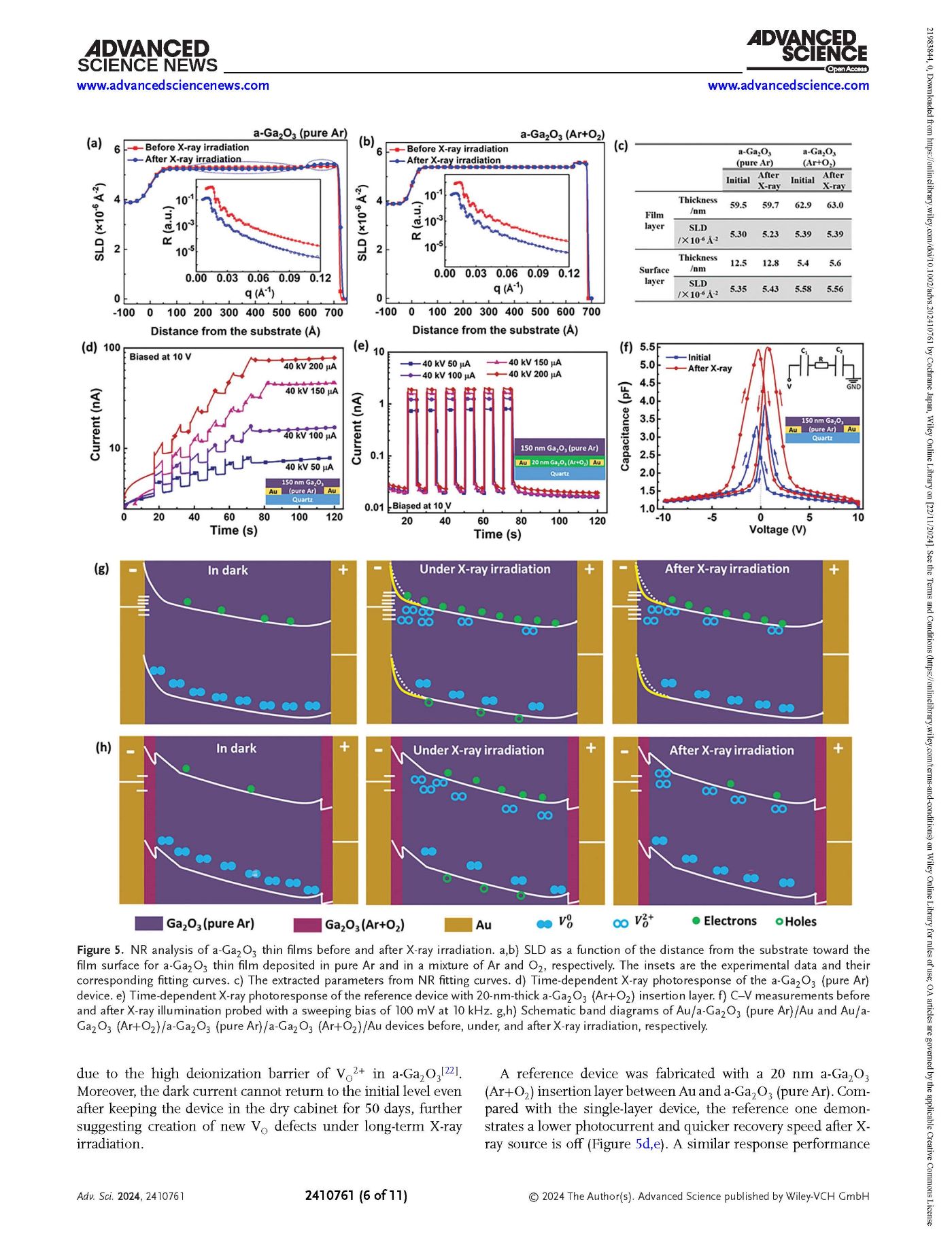
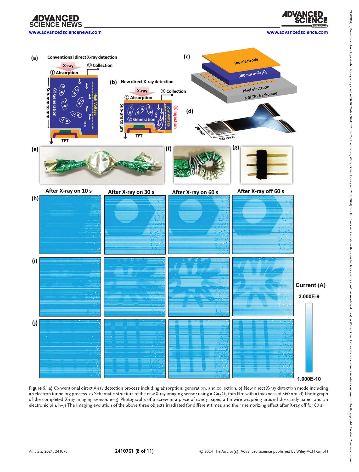
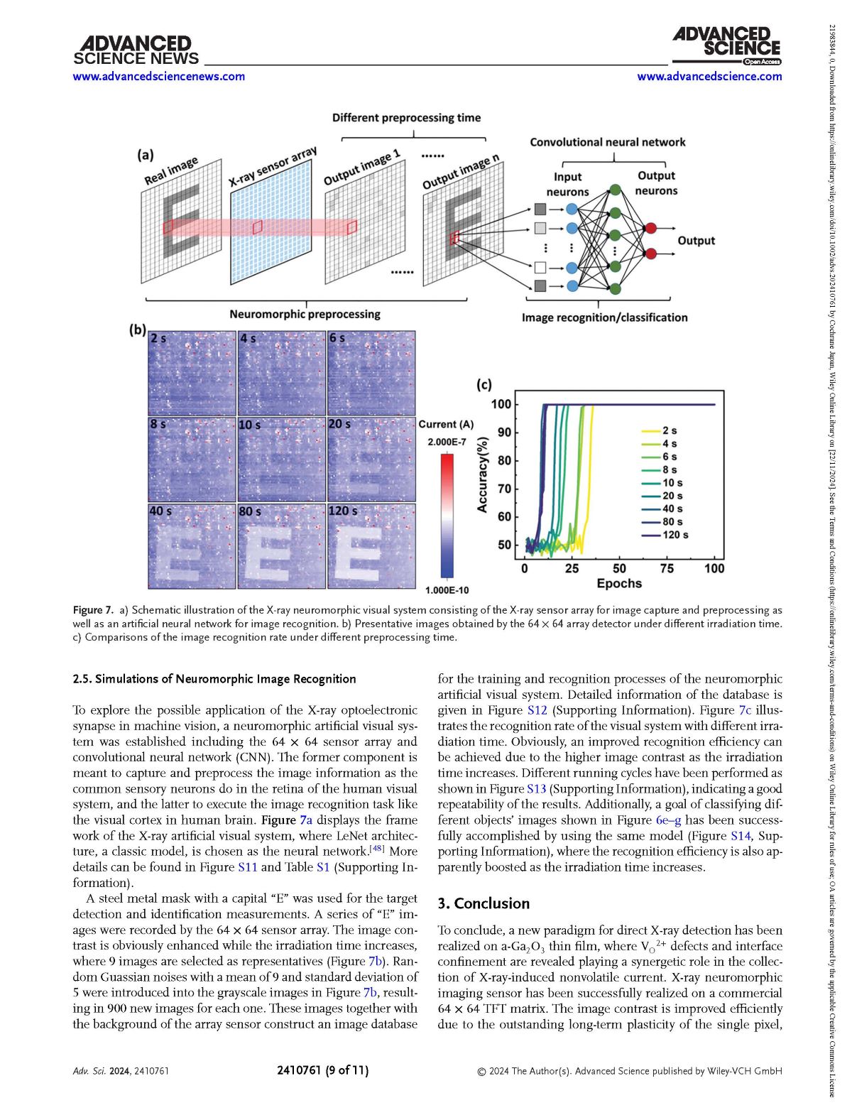
Machine vision techniques are widely applied for object identification in daily life and industrial production, where images are captured and processed by sensors, memories, and processing units sequentially. Neuromorphic optoelectronic synapses, as a preferable option to promote the efficiency of image recognition, are hotly pursued in non-ionizing radiation range, but rarely in ionizing radiation including X-rays. Here, the study proposes an X-ray optoelectronic synapse using amorphous Ga2O3 (a-Ga2O3) thin film. Boosted by the interfacial VO2+ defects and its slow neutralization rate, the enhanced electron tunneling process at metal/a-Ga2O3 interface produces remarkable X-ray-induced post-synaptic current, contributing to a sensitivity of 20.5, 64.3, 164.1 µC mGy−1 cm−2 for the 1st, 5th, and 10th excitation periods, respectively. Further, a 64 × 64 imaging sensor is constructed on a commercial amorphous Si (a-Si) thin film transistor (TFT) array. The image contrast can be apparently improved under a series of X-ray pulses due to an outstanding long-term plasticity of the single pixel, which is beneficial to the subsequent image recognition and classification based on artificial neural network. The merits of large-scale production ability and good compatibility with modern microelectronic techniques belonging to amorphous oxide semiconductors may promote the development of neuro-inspired X-ray imagers and corresponding machine vision systems.
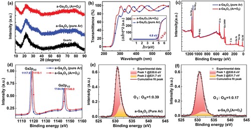
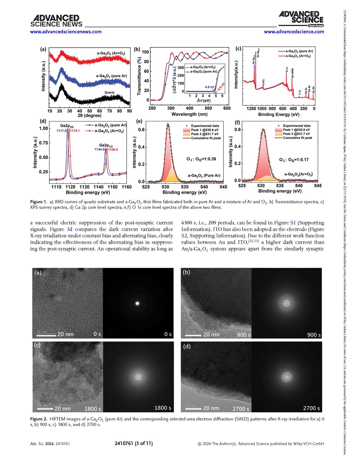
Figure 1.a) XRD curves of quartz substrate and a-Ga2O3 thin films fabricated both in pure Ar and a mixture of Ar and O2. b) Transmittance spectra, c) XPS survey spectra, d) Ga 2p core level spectra, e,f) O 1s core level spectra of the above two films.
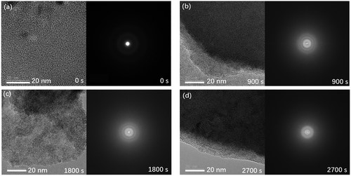
Figure 2.HRTEM images of a-Ga2O3 (pure Ar) and the corresponding selected area electron diffraction (SAED) patterns after X-ray irradiation for a) 0 s, b) 900 s, c) 1800 s, and d) 2700 s.
DOI:
doi.org/10.1002/advs.202410761
