Paper Sharing
【International Papers】Unveiling the synergic potential of dual junction MoSe₂/n-Ga₂O₃/p-GaN heterojunctions for ultra-broadband photodetection
日期:2025-01-15阅读:937
Researchers from the CSIR-National Physical Laboratory have published a dissertation titled "Unveiling the synergic potential of dual junction MoSe2/n-Ga2O3/p-GaN heterojunctions for ultra-broadband photodetectio" in Materials Advances.
Abstract
For practical optoelectronic applications, photodetectors capable of detecting light across a wide wavelength range (200–1100 nm) are essential. Heterojunction semiconductors play a crucial role in developing such multi-wavelength photodetectors. In particular, the heterojunction of transition metal chalcogenides (tuneable bandgap and high electron mobility) and Ga2O3 (wide bandgap of >4 eV) is a significant research topic for photodetector fabrication exhibiting an ultrawide spectral photodetection capability. In this study, epitaxial β-Ga2O3 thin films were grown on atomically flat sapphire (0001) and p-GaN/sapphire (0001) surfaces using a pulsed laser deposition technique. The effect of the substrate on the crystalline, optical, electronic, and photoresponse properties of β-Ga2O3 thin films was thoroughly investigated and correlated with theoretical insights from density functional theory. To achieve broadband photodetection, a heterojunction of MoSe2 and the as-grown Ga2O3 films was fabricated, enabling light detection from the deep ultraviolet (UV) to the near-infrared (NIR) spectral regions. The MoSe2/Ga2O3/p-GaN device exhibited an expanded detection range from deep ultraviolet (240–320 nm) to long-wavelength ultraviolet (320–400 nm) and a significant responsivity of 5.5 A W−1 in the NIR region, nearly fourfold higher than that of the MoSe2/Ga2O3/sapphire device. These results highlight the potential of these hybrid structures for developing multi-wavelength photodetectors with high photoresponse across the deep-UV to NIR spectral regions, offering promising applications in fields ranging from environmental monitoring to communications.

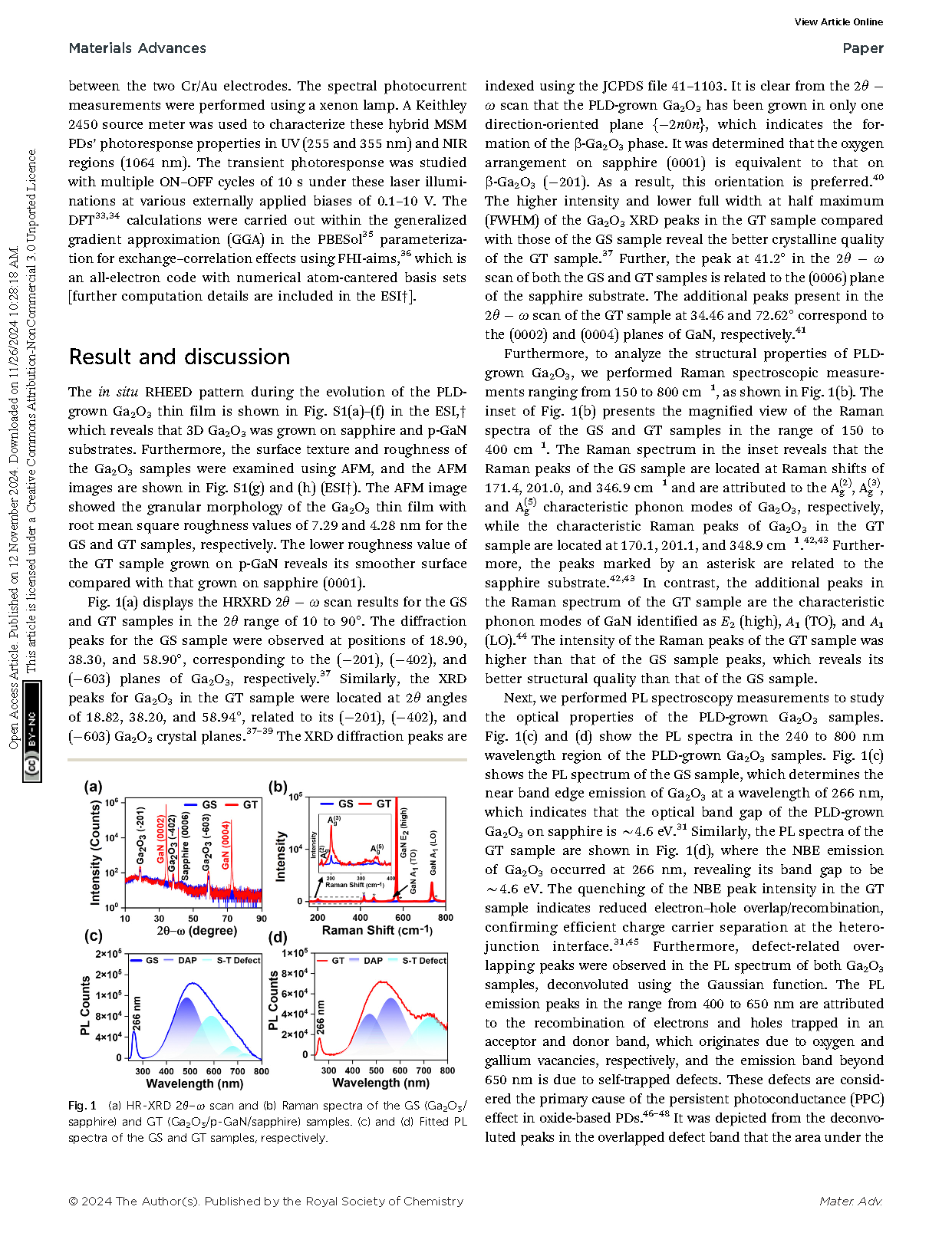
Fig. 1 (a) HR-XRD 2θ–ω scan and (b) Raman spectra of the GS (Ga2O3/sapphire) and GT (Ga2O3/p-GaN/sapphire) samples. (c) and (d) Fitted PL spectra of the GS and GT samples, respectively.

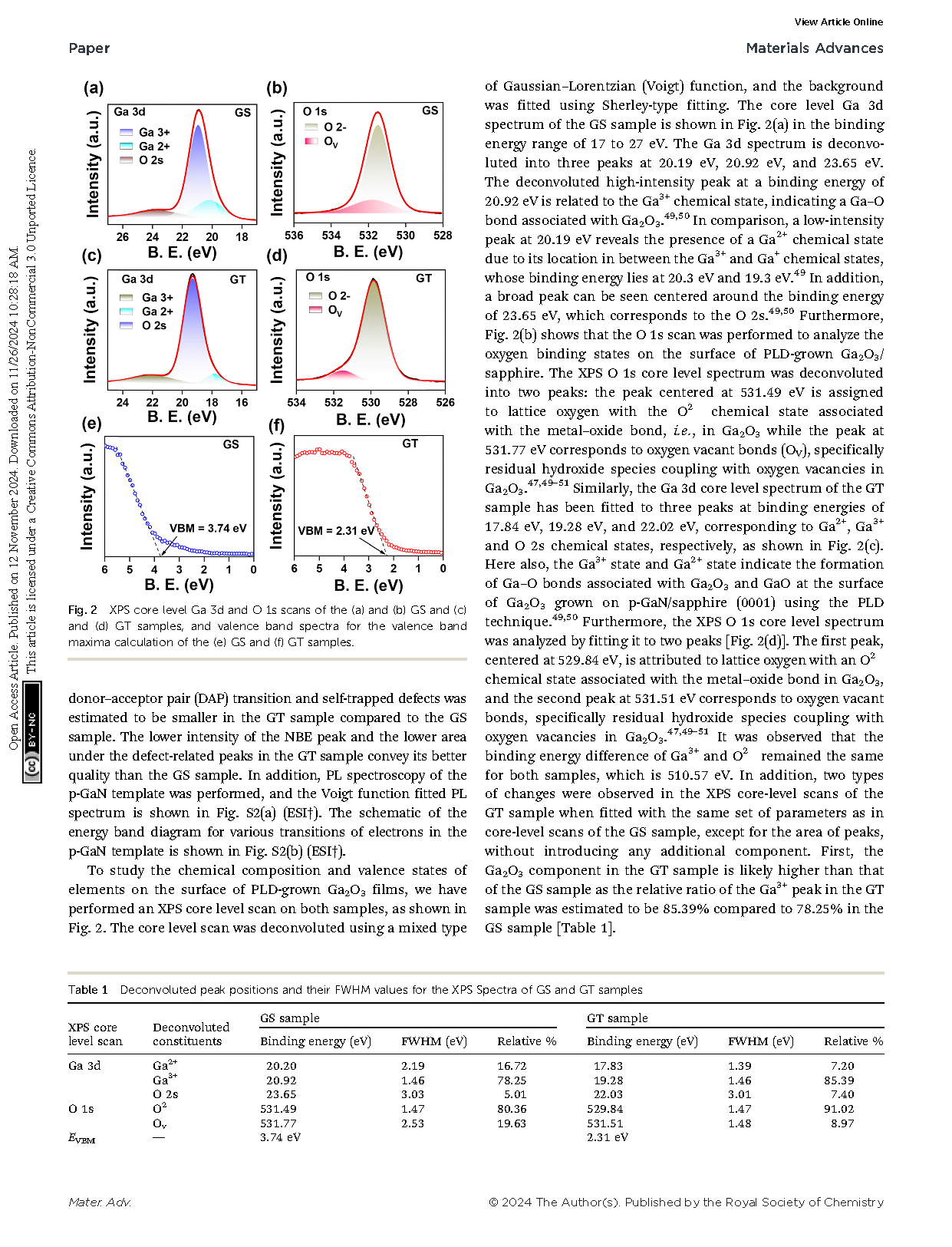
Fig. 2 XPS core level Ga 3d and O 1s scans of the (a) and (b) GS and (c) and (d) GT samples, and valence band spectra for the valence band maxima calculation of the (e) GS and (f) GT samples.
DOI:
doi.org/10.1039/D4MA00934G