


Paper Sharing
【Member Papers】Lu Xiaoli & He Yunlong et al.: The In-Situ Parasitic Microstructure Interface and Defect Formation Mechanism in (010) β-Ga₂O₃ Epitaxial Film via MOCVD
日期:2025-01-22阅读:1097
Recently, Professor Lu Xiaoli and Associate Professor He Yunlong of Xidian University and Associate Professor Wang Zhan of Xi 'an University of Posts and Telecommunications published a research paper in Science China Materials, systematically analyzing the morphology, structure and formation mechanism of interfacial defect in (010) β-Ga2O3 film grown by MOCVD.
Key Points of the Paper
1) The observed defects exhibit a polygonal shape with a ridge-like hillock along the [001] direction. Transmission electron microscopy (TEM) microanalysis reveals that polygonal hillock defects are composed of twin grains forming an inverted pyramid shape embedded in the epitaxial layer, which exhibits twofold rotational symmetry along the [100] crystal direction. The boundary between the defective and perfect lattices appears band-like, characterized by complex faults, with structural relationships between the twin region and the matrix identified as [001] matrix∥[010]Defect and {−310}matrix∥{−201}Defect.
2) The origin of surface defects in the (010) β-Ga2O3 homoepitaxial layers could be attributed not only to the extent of substrate defects but also to epitaxial process conditions.
3) The definitive explanation is the localized aggregation of gallium atoms/oxygen vacancies during the growth process, as evidenced by energy-dispersive X-ray (EDX) analysis and optimized experiments.
This work provides brand-new perspectives into the study of defects in β-Ga2O3 epitaxial films, which further advances the application of Ga2O3 materials in power device technologies.
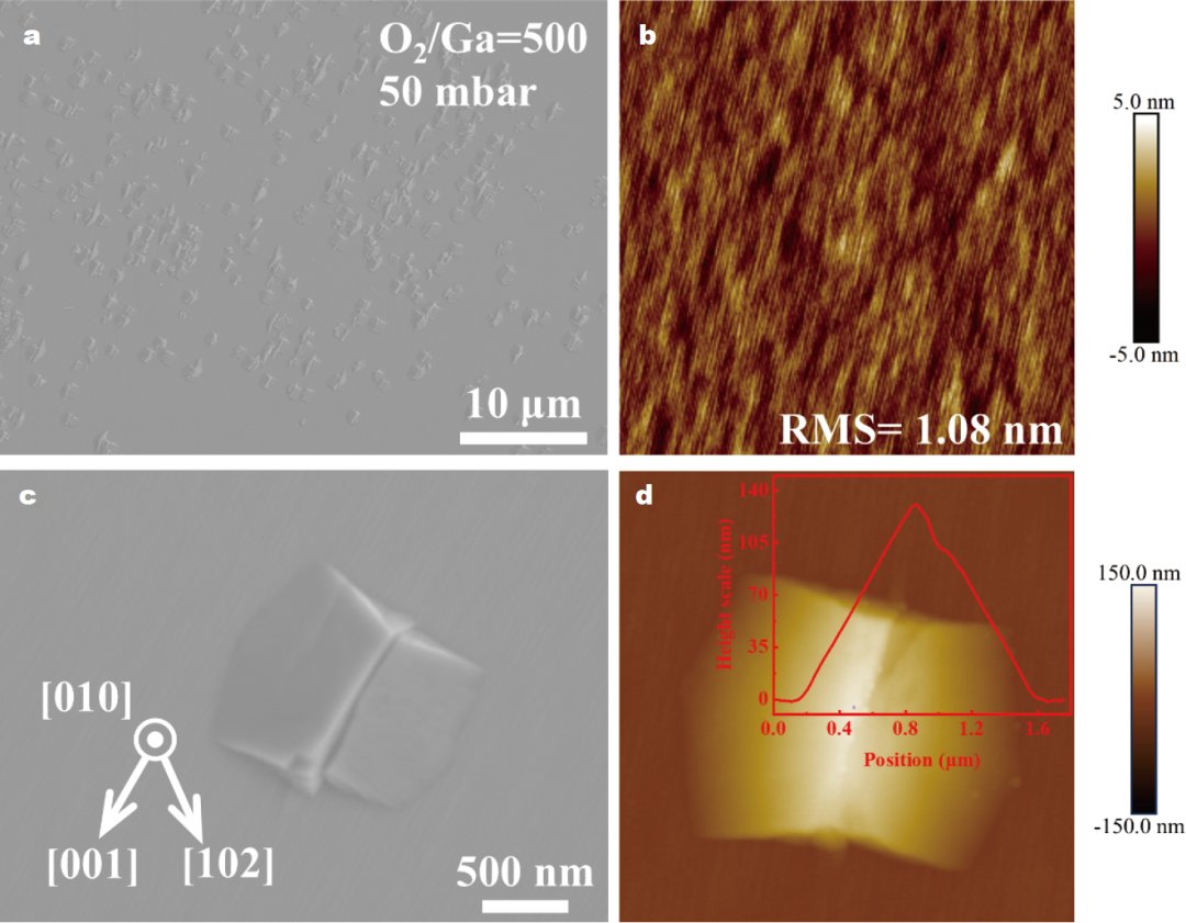
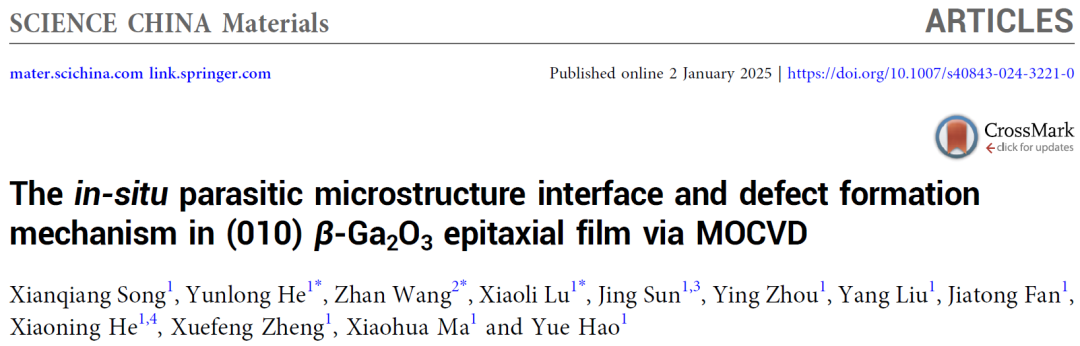
Figure 1. (a) SEM image of the surface of (010) β-Ga2O3 homoepitaxial film with dense polygonal hillock defects. (b) AFM image of an area (5 μm × 5 μm) without defects. (c) High-magnification SEM image of a polygonal hillock defect. (d) AFM image and the height profile of a polygonal hillock defect.
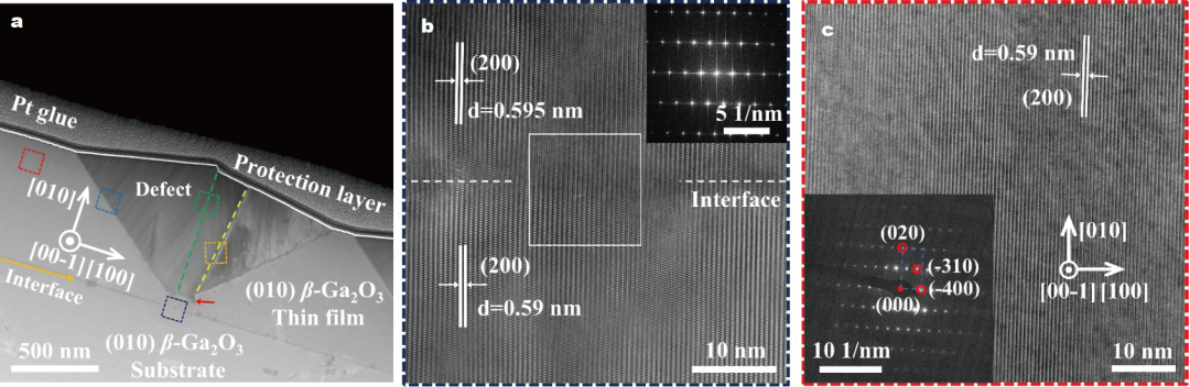
Figure 2. (a) Cross-sectional TEM image of a polygonal hillock defect. (b) HRTEM image of the film-substrate interface, highlighted by the dark blue dashed box in (a). (c) HRTEM image of β-Ga2O3 homoepitaxial layer indicated by the red dashed box in (a), and the inset shows the selected electron diffraction pattern.
Figure 3. (a) HRTEM image at the boundary of the twin inside the polygonal hillock defect marked by the green dashed line box in Fig. 2a. (b) Diffraction pattern showing [010] orientation circled in blue and [0−10] orientation circled in red, with hklL and hklR exhibiting mirror symmetry. (c) A stick and ball model of the observed twin boundary. Bright green and red balls correspond to Ga and O atoms, respectively.
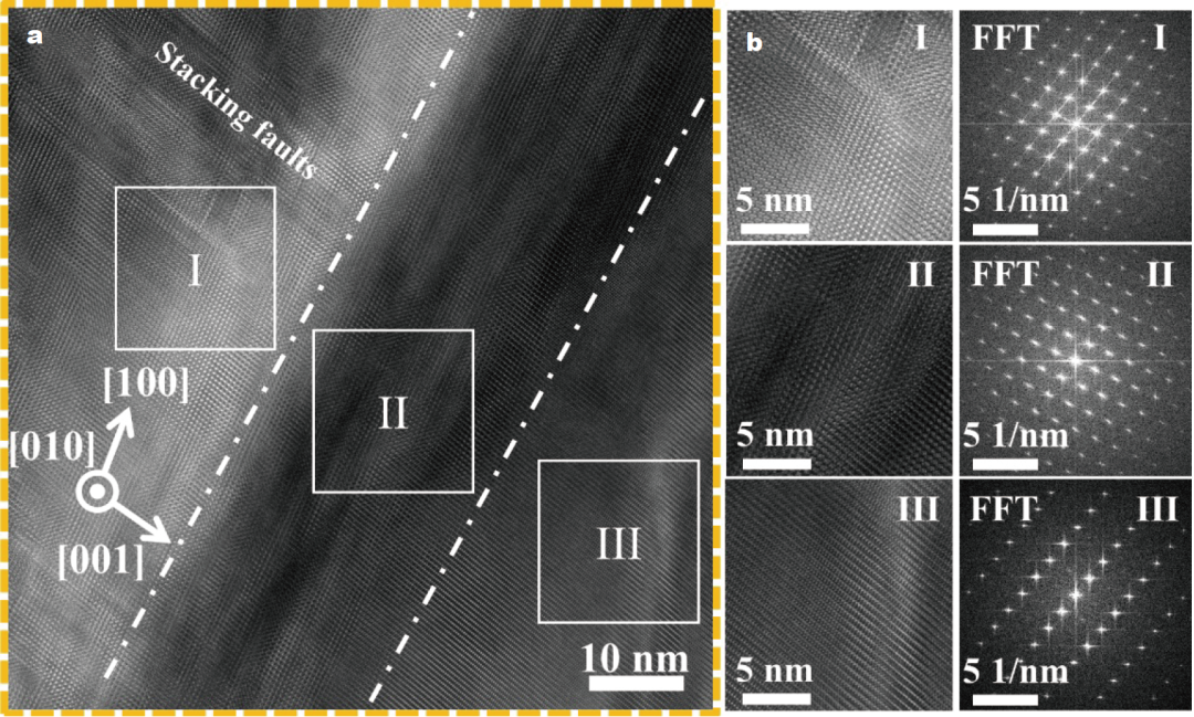
Figure 4. (a) HRTEM image of the yellow boxed area in Fig. 2a, in which there exists a boundary that divides the right twin region into two parts. (b) Enlarged image and FFT pattern of regions I, II and III.
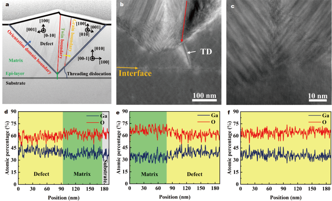
Figure 5. (a) Schematic cross section of the polygonal hillock defect. (b) Magnified TEM image and (c) HRTEM image of the bottom area of the polygonal hillock defect. The STEM-EDX quantification line profiles (d) at the interface between the matrix and the defect, (e) at the boundary studied in Fig. 4, and (f) at the bottom of the defect show the atomic percentages of Ga (blue) and O (red), and the specific scanning positions are indicated by green, blue, and yellow arrows in (a).
Article Information
Xianqiang Song, Yunlong He, Zhan Wang, Xiaoli Lu, Jing Sun, Ying Zhou, Yang Liu, Jiatong Fan, Xiaoning He, Xuefeng Zheng, Xiaohua Ma, Yue Hao. The in-situ parasitic microstructure interface and defect formation mechanism in (010) β-Ga2O3 epitaxial film via MOCVD. Sci. China Mater. (2024).
https://doi.org/10.1007/s40843-024-3221-0
