Paper Sharing
【Member Papers】Yang Ming Chiao Tung University——Study of thermal annealing on gallium oxide heteroepitaxial layers grown on SiC for vertical Schottky barrier diodes applications
日期:2025-02-08阅读:862
Researchers from the Yang Ming Chiao Tung University have published a dissertation titled "Study of thermal annealing on gallium oxide heteroepitaxial layers grown on SiC for vertical Schottky barrier diodes applications" in Applied Surface Science Advances.
Abstract
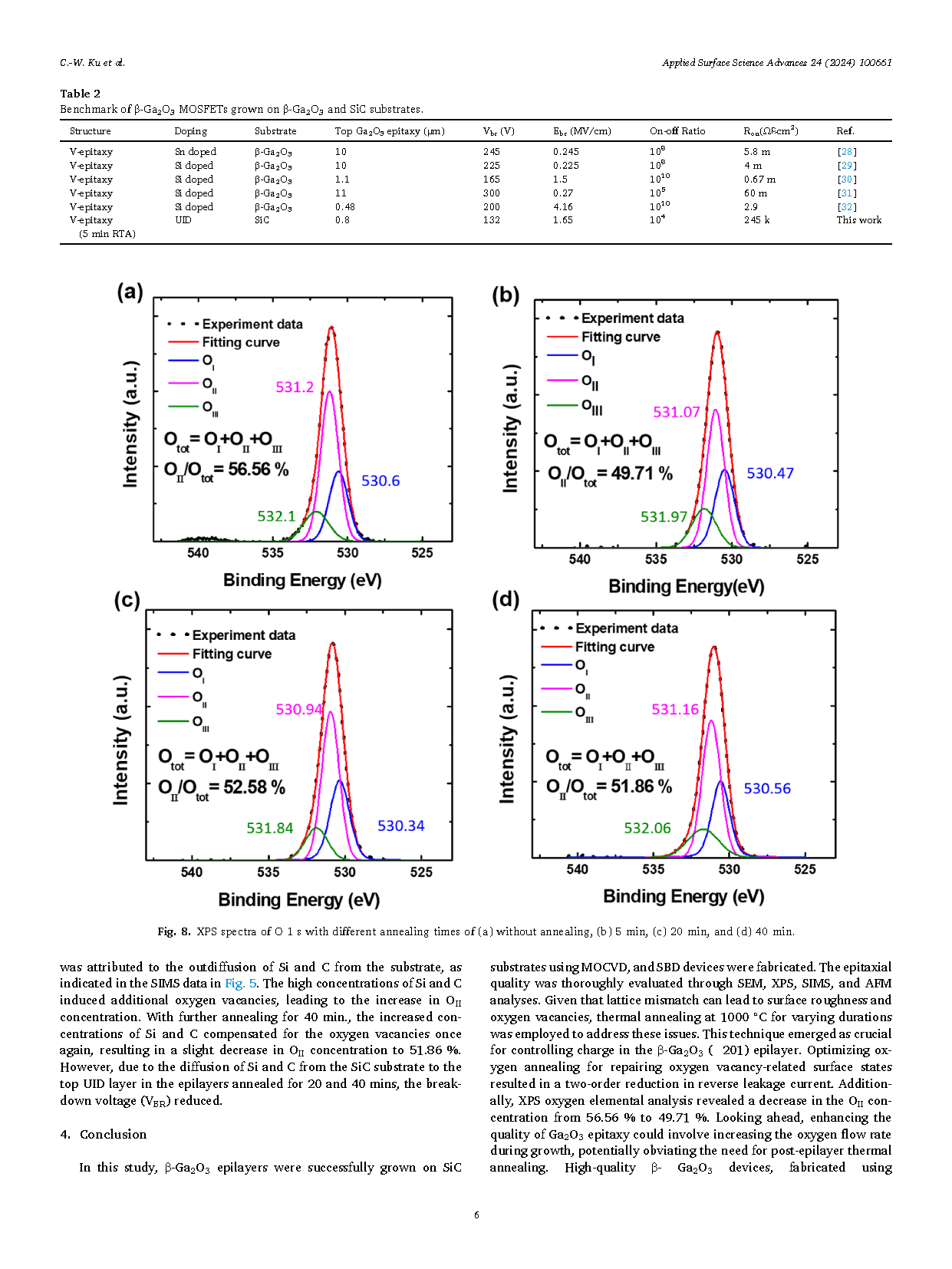
This study successfully grew ꞵ-Ga2O3 epitaxial films on silicon carbide substrates by metalorganic chemical vapor deposition and fabricated vertical Schottky barrier diodes (SBDs), which were annealed in a high temperature furnace. The high surface roughness and oxygen vacancies of the unannealed device caused a large leakage current, thus three different annealing durations were used to repair the surface oxygen vacancies in an O2:N2=1:4 gas environment. The results showed that a 5-minute thermal annealing process was the most effective in repairing surface oxygen vacancies. According to the X-ray photoelectron spectroscopy spectra of the O 1 s core levels in Ga2O3 epilayers, the proportion of oxygen vacancies decreased from 56.56 % to 49.71 %. Additionally, the leakage current density was decreased from 10−3 to 10−5 A/cm2 and the surface roughness decreases to 32.6 nm due to stress release. Furthermore, the barrier heights (φb) of the SBDs without annealing, and after annealed for 5, 20, and 40 min were measured at 0.911, 1.229, 1.090, and 1.115 eV, respectively. It was observed that the SBD fabricated on the epilayer annealed for 5 min exhibited the lowest leakage current (approximately 2 × 10⁻⁵ A/cm²) and the highest breakdown voltage, measuring around 132 V.
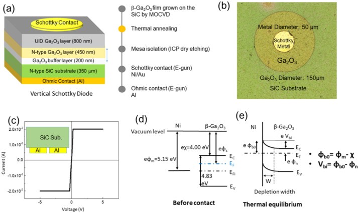
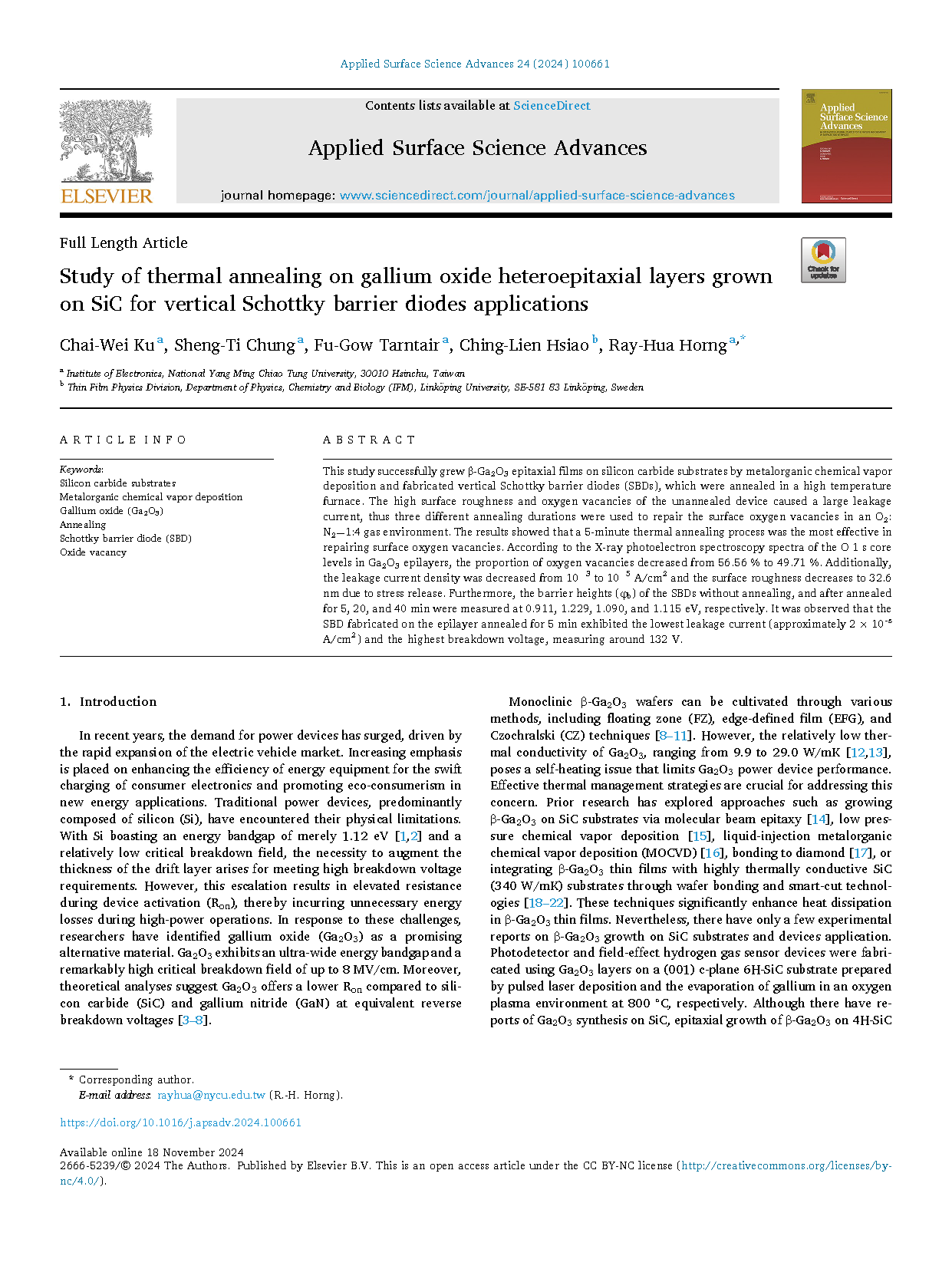
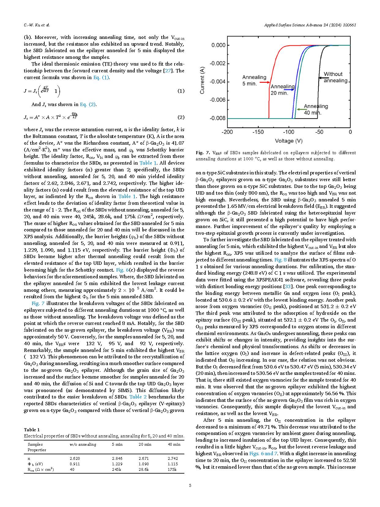
Fig. 1. (a) Schematic structure of SBD made of Ga2O3 grown on SiC substrate with fabrication flow chat, (b) a photograph or SEM image of the fabricated device, (c) I-V curve measured from the Al pads, and theoretical band diagrams of Ni and Ga2O3 (d) before and (e) after contact.
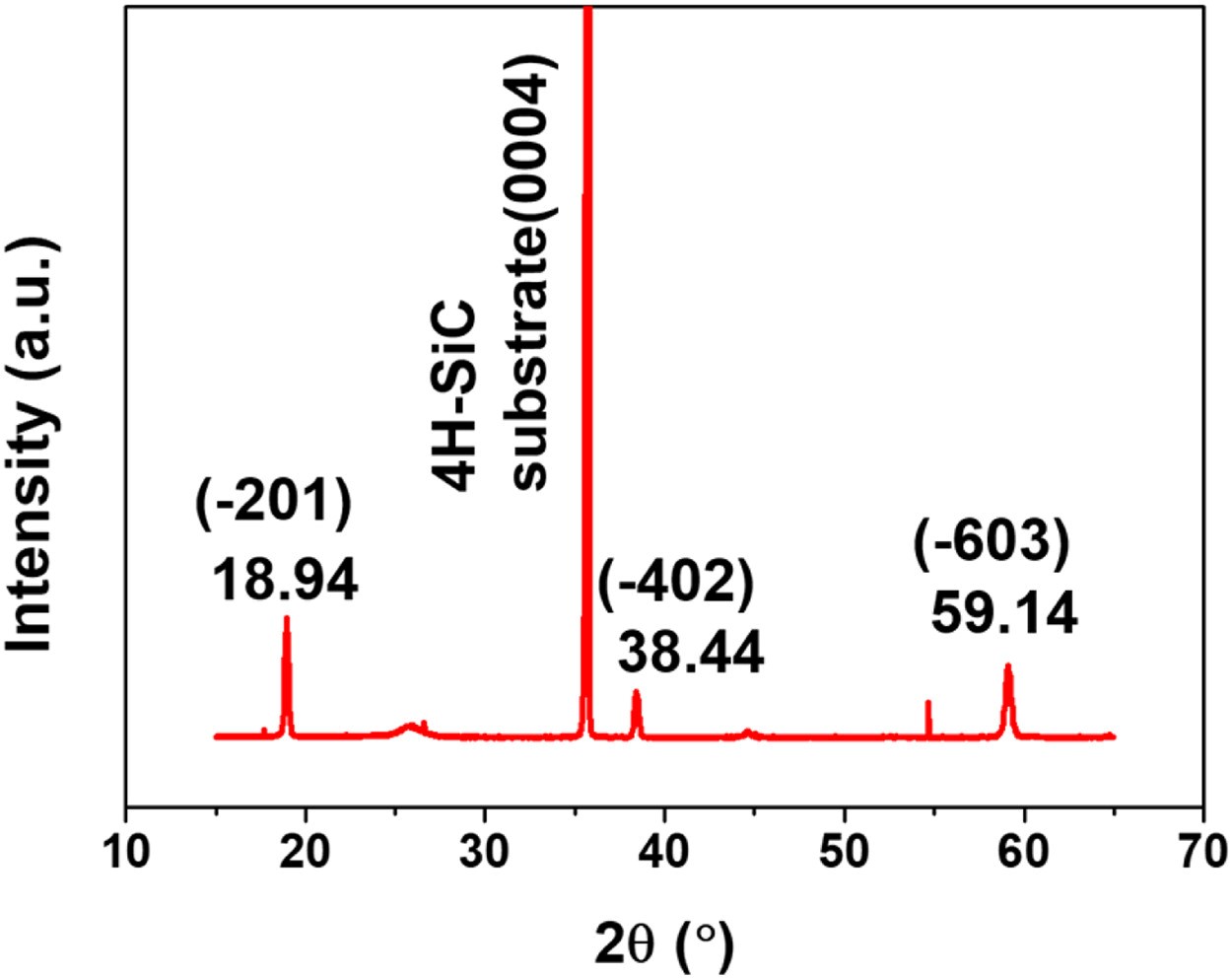
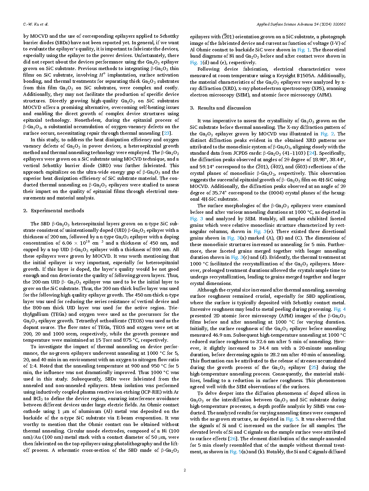
Fig. 2. XRD pattern of the MOCVD-grown β-Ga2O3 epilayer on SiC substrate.
DOI:
doi.org/10.1016/j.apsadv.2024.100661