Paper Sharing
【Member Papers】GAREN SEMI's Breakthrough in Gallium Oxide Single Crystal Growth were Published in the Crystal Growth&Design
日期:2025-02-11阅读:954
Recently, Hangzhou GAREN SEMI and the research team of Zhejiang University have made key technological breakthroughs in the field of β-Gallium Oxide (β-Ga2O3) single crystal growth! Published in Volume 25 / Issue 3 of the internationally renowned journal Crystal Growth & Design entitled " Highly Coherent Grain Boundaries Induced by Local Pseudomirror Symmetry in β-Ga2O3 ”
β-Ga2O3 is a kind of material which is easy to produce twins in the growth and epitaxy of single crystal, which seriously restricts the improvement of the yield of single crystal growth and epitaxy. Based on the Symmetry principle, this study proposed Pseudo Symmetry in β-Ga2O3 for the first time, successfully analyzed the physical origin of the (100) twin boundary and the "Coherent Asymmetric Grain Boundaries", and solved the "gene" that makes β-Ga2O3 easy to form twins. It is helpful to improve the yield of single crystal growth and epitaxy from the level of scientific principle and engineering design, and clear the key obstacles for the development of high-performance devices.
With reference to the research results, the R&D team of GAREN carried out optimization and iteration of the β-Ga2O3 growth process based on the self-developed Gallium Oxide special equipment, which initially solved the problem of twins in the industry.
1.Article Guide
Symmetry is one of the core concepts of the macro world. Everything from the conservation of angular momentum in the motion of celestial bodies to the form and function of natural organisms is deeply influenced by symmetry. Even at the more microscopic atomic scale, symmetry is essential. A good understanding of crystalline materials also requires a good understanding of their symmetry, and β-Ga2O3 is no exception.
β-Ga2O3 is a kind of wide band gap semiconductor material with wide application prospect. It is well known that the space group of β-Ga2O3 is C2/m, which has fewer symmetric operations than the 4H-SiC and GaN with the P63mc space group. In the β-Ga2O3 cell shown in Figure 1, there are (010) planes with specular symmetry and [010] crystal orientation with quadratic and helical rotation symmetries.
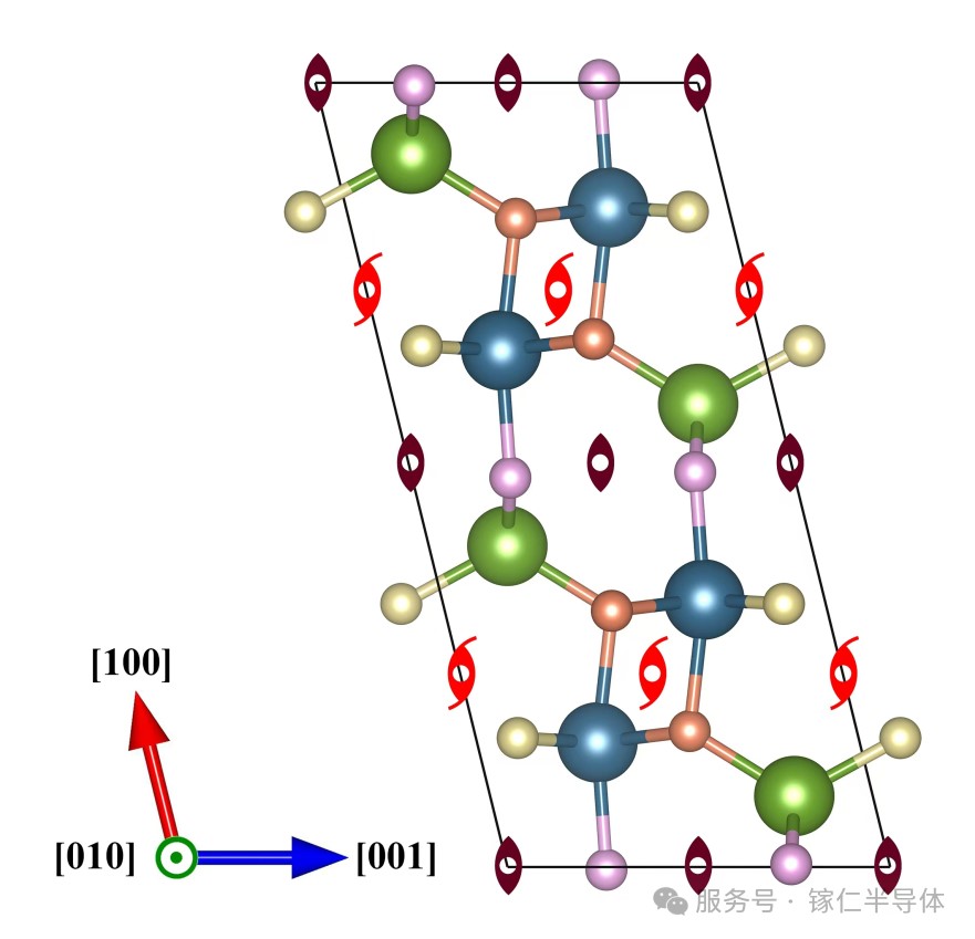
[Figure 1] Standard symmetry in a β-Ga2O3 cell
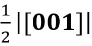
However, in addition to the strict symmetries described above, β-Ga2O3 also has special "Pseudo Symmetry". As shown in Figure 2 (a), β-Ga2O3 has an atomic layer structure of "quasi-specular symmetry," meaning that the position between the mirror image of the layer's atoms and itself does not strictly coincide, but is separated by only a negligible distance. The "quasi specular symmetry" plane of this atomic layer is perpendicular to the (100) plane, marked as a black dashed line in Figure 2 (a), and the spacing of this " pseudo symmetry plane" is:
This "pseudo symmetry" makes the growth and epitaxy of single crystal of β-Ga2O3 prone to (100) face twins. As shown in Figure 2 (b), after the formation of the twin structure, there is almost no atomic displacement and bond distortion at the twin interface, and the twin boundary energy is only 0.008J/m2 -- almost no!
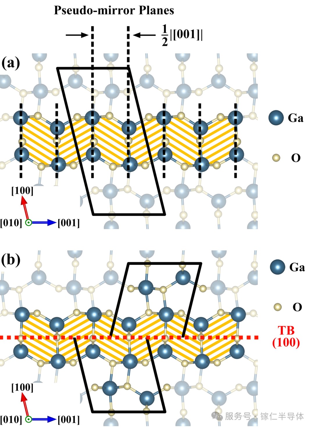
[Figure 2] (a) pseudo symmetric atomic layer in β-Ga2O3; (b) the (100) face twin of β-Ga2O3 built on the pseudo symmetry
At this point, another coincidence appears: there is a special "lattice coincidence" in the single-cell structure of β-Ga2O3, as shown in Figure 3 (a) :

This "lattice coincidence" is superimposed with "pseudo-symmetry" so that there are two special "twin cores" in β-Ga2O3, as shown in Figure 3 (b) and (c).
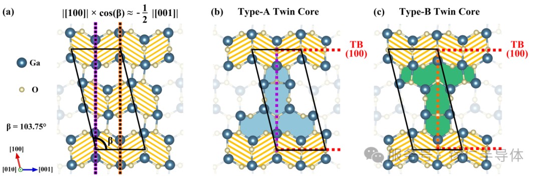
[Figure 3] (a) Special "lattice coincidences" in β-Ga2O3; (b) A-type twin core in β-Ga2O3; (c) B-type twin core in β-Ga2O3
A three-dimensional extension of the " twinning core" in Figure 3 (b) and (c) constitutes the series of twin boundary structures in Figure 4. On a microcosmic level, they can be viewed as twin chains strung by twin cores; On a macroscopic level, these interface structures appear as twins composed of different crystal face.
For example, the interface structure in Figure 4 (b) shows that the (002) and (20-2) faces of β-Ga2O3 produce twins on a macro level! Here, we name it "Coherent Asymmetric Grain Boundaries" (CAGBs).
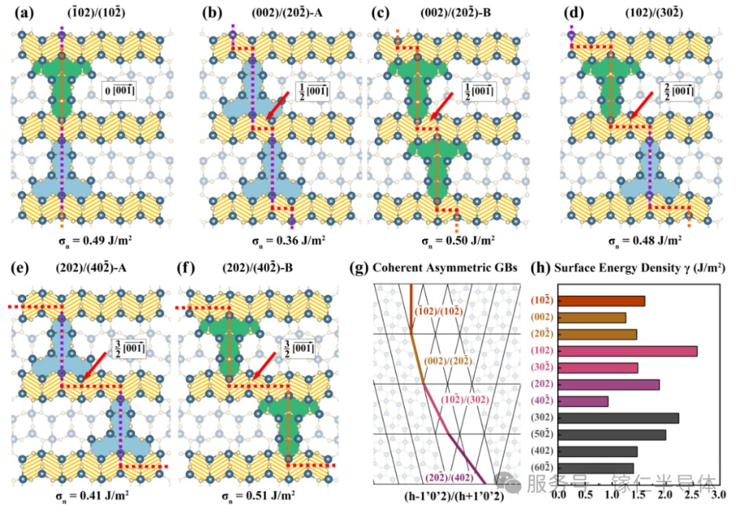
[Figure 4] (a) - (f) The twin core is expanded into a three-coherent asymmetric twin; (g) coherent asymmetric twins are macroscopically presented as twin boundaries composed of two different crystal face; (f) The surface energy of the crystal face constituting a coherent asymmetric twin
Coherent Asymmetric Grain Boundaries plays an important role in the growth and epitaxy of single crystal of β-Ga2O3. As shown in Figure 5, when growing 2-inch β-Ga2O3 single crystal by CZ method, we observed the structure of the symmetrical asymmetric twin, and determined that Figure 4 (b) was the most stable β-Ga2O3 coherent asymmetric twin structure through the HAADF-STEM and first-principles calculations in Figure 5 (e).
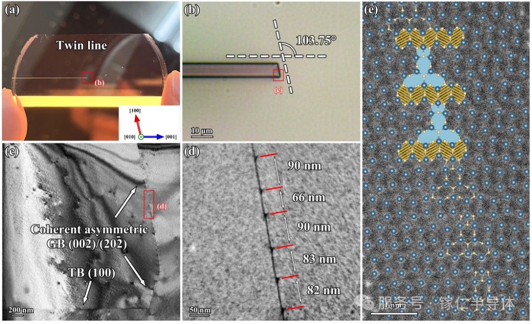
[Figure 5] Coherent asymmetric twins in 2-inch β-Ga2O3 single crystal grown by Cz method were used by (a) Polarizing strain gauge; (b) optical microscope; (c) TEM; (d) the structure of coherent asymmetric twins observed by STEM and (e) HAADF-STEM.
We take the step flow epitaxy of β-Ga2O3 (100) surface substrate as an example to illustrate the important role of coherent asymmetric twins on β-Ga2O3 epitaxy. A large number of studies have shown that the β-Ga2O3 (100) surface can achieve step flow growth through chamfer to improve epitaxial quality. However, the principle that the chamfer direction plays a decisive role in epitaxial mass remains unresolved (APL Mater. 7 022515 (2019)). Here, we need to emphasize the critical role of Coherent Asymmetric Grain Boundaries.
As shown in Figure 6 (a), the (100) substrate chamfer exposes the step face of (001) along [001] and the chamfer exposes the step face of (-201) along [00-1]. At the (001) step surface exposed along the [001] chamfer, a twin defect is formed due to the presence of coherent asymmetric twins. Its energy density is 3.11J/m2, which is even lower than the 3.26J/m2 energy density of the defect without twins - which means that during epitaxy, twins form spontaneously! However, on the (100) substrate chamfer along [00-1], the (-201) step surface inhibits the formation of associated twin defect. Therefore, in order to improve the quality of epitaxy, it is essential to choose the direction of β-Ga2O3 substrate reasonably.
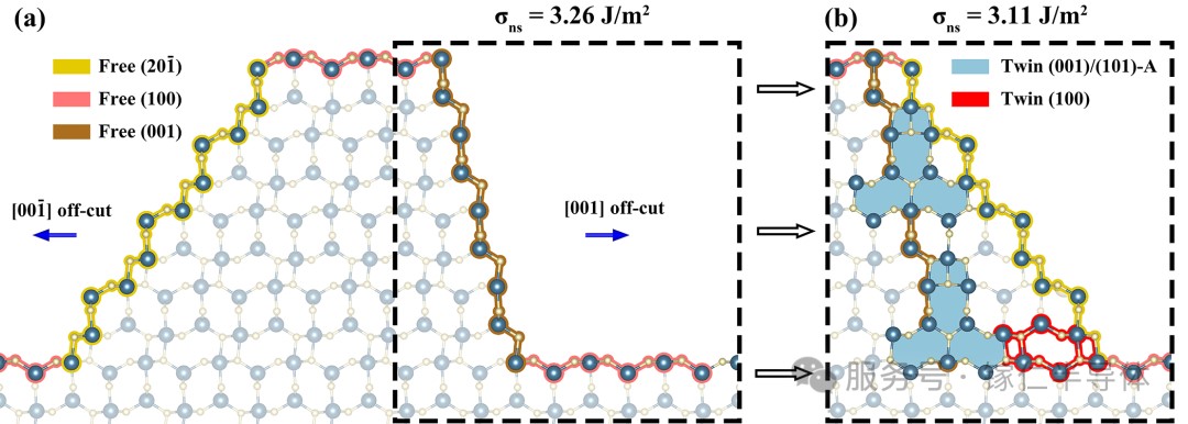
[Figure 6] (a) β-Ga2O3 (100) substrate chamfer exposes (001) step face along [001] direction and chamfer exposes (-201) step face along [00-1] direction. (b) On the (001) step surface, the defect of the twin at the step caused by a coherent asymmetric twin are lower in energy than the step without defect.
2.Summary
In this groundbreaking research achievement, GAREN SEMI and the research team of Zhejiang University proposed the theory of " pseudo symmetry " and "lattice coincidence" for the first time, and by in-depth analysis of the physical mechanism of the twin boundary, successfully overcome the long-term problem of crystal defect in the industry, and realized the mass production of 2-inch (010) surface twinless β-Ga2O3 substrate. Marks a new level of China's scientific and engineering strength in the field of wide band gap semiconductor.
Looking forward to the future, GAREN SEMI will continue to promote the development of the national wide band gap semiconductor industry, deepen scientific and technological innovation in the field of Gallium Oxide, provide customers with high-quality and cost-effective Gallium Oxide products, and strive to be a technology leader in the industry.
For more details, please read the original article
(DOI: 10.1021/acs.cgd.4c01504)
Company Profile
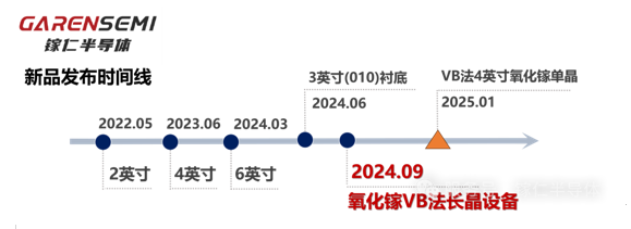
Hangzhou GAREN SEMI Co., Ltd. was established in September 2022, is a technology enterprise focusing on the research and development, production and sales of Gallium Oxide and other semiconductor materials. The company has created a new technology for Gallium Oxide single crystal growth, and has 14 international and domestic invention patents, breaking through the monopoly and blockade of Western countries such as the United States and Japan on Gallium Oxide substrate materials. Based on solving the major national needs, GAREN SEMI will be deeply engaged in the continuous innovation of the Gallium Oxide upstream industry chain, and strive to provide product guarantee for the development of China's power electronics and other industries.
GAREN SEMI leads the industry innovation, adopts the self-developed casting method Gallium Oxide single crystal growth technology, realizes the production technology breakthrough of 6-inch single crystal substrate and wafer-level (010) single crystal substrate, and develops the first Gallium Oxide special VB crystal growth equipment including process package. The company has mastered the core technology of Gallium Oxide growth, processing, epitaxy and other whole chain, providing customers with large-scale high-quality Gallium Oxide products and equipment with complete independent intellectual property rights.
For more information about GAREN SEMI and its products
Please visit our official website: http://garen.cc/
Or contact us:
Mr. Jiang :15918719807
Email: jiangjiwei@garen.cc
Mr. Xia :19011278792
Email:xianing@garen.cc