Paper Sharing
【International Papers】Electrothermal enhancement of β-(AlₓGa₁₋ₓ)₂O₃/Ga₂O₃ heterostructure field-effect transistors via back-end-of-line sputter-deposited AlN layer
日期:2025-02-13阅读:832
Researchers from the U.S. Naval Research Laboratory have published a dissertation titled "Electrothermal enhancement of β-(AlxGa1−x)2O3/Ga2O3 heterostructure field-effect transistors via back-end-of-line sputter-deposited AlN layer" in Journal of Applied Physics.
Abstract
The electrothermal device performance of β-(Al0.21Ga0.79)2O3/Ga2O3 heterostructure field-effect transistors (HFETs) was enhanced by incorporating a 400 nm thick AlN capping layer via back-end-of-line room-temperature reactive sputter deposition. The AlN-capped HFETs demonstrated DC power densities >5 W/mm, higher than any previous report on lateral β-Ga2O3 transistors on native substrates. The breakdown voltage (VB) of the uncapped HFETs was 569 ± 250 V with a maximum VB of 947 V. For the AlN-capped HFETs, VB increased to 1210 ± 351 V with a maximum VB of 1868 V. The AlN-capped HFETs demonstrated a 27% reduction in device-level thermal resistance (RTH) as measured from the gate electrode. The combined use of electrical and thermal simulation helped elucidate the coupled electrothermal contributions to the measured reduction in the temperature rise for the AlN-capped HFETs. Although the measured AlN film thermal conductivity (13.3 ± 1.3 W/mK) was comparable to that of bulk β-Ga2O3, the capping layer still reduced the simulated peak channel temperature rise by ∼4% due to heat spreading only. Electrical simulation revealed that electric field spreading was an additional mechanism that contributed to the majority of the simulated 18% reduction in the peak channel temperature rise through delocalization and redistribution of the heat generation in the channel. Thermal modeling was used to evaluate further improvements in thermal performance that can be realized by optimizing the sputter deposition process to achieve thicker and higher thermal conductivity AlN.
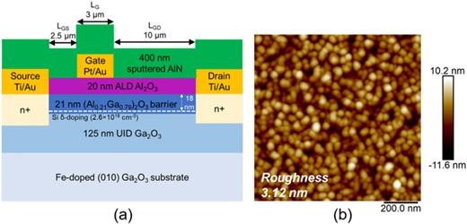
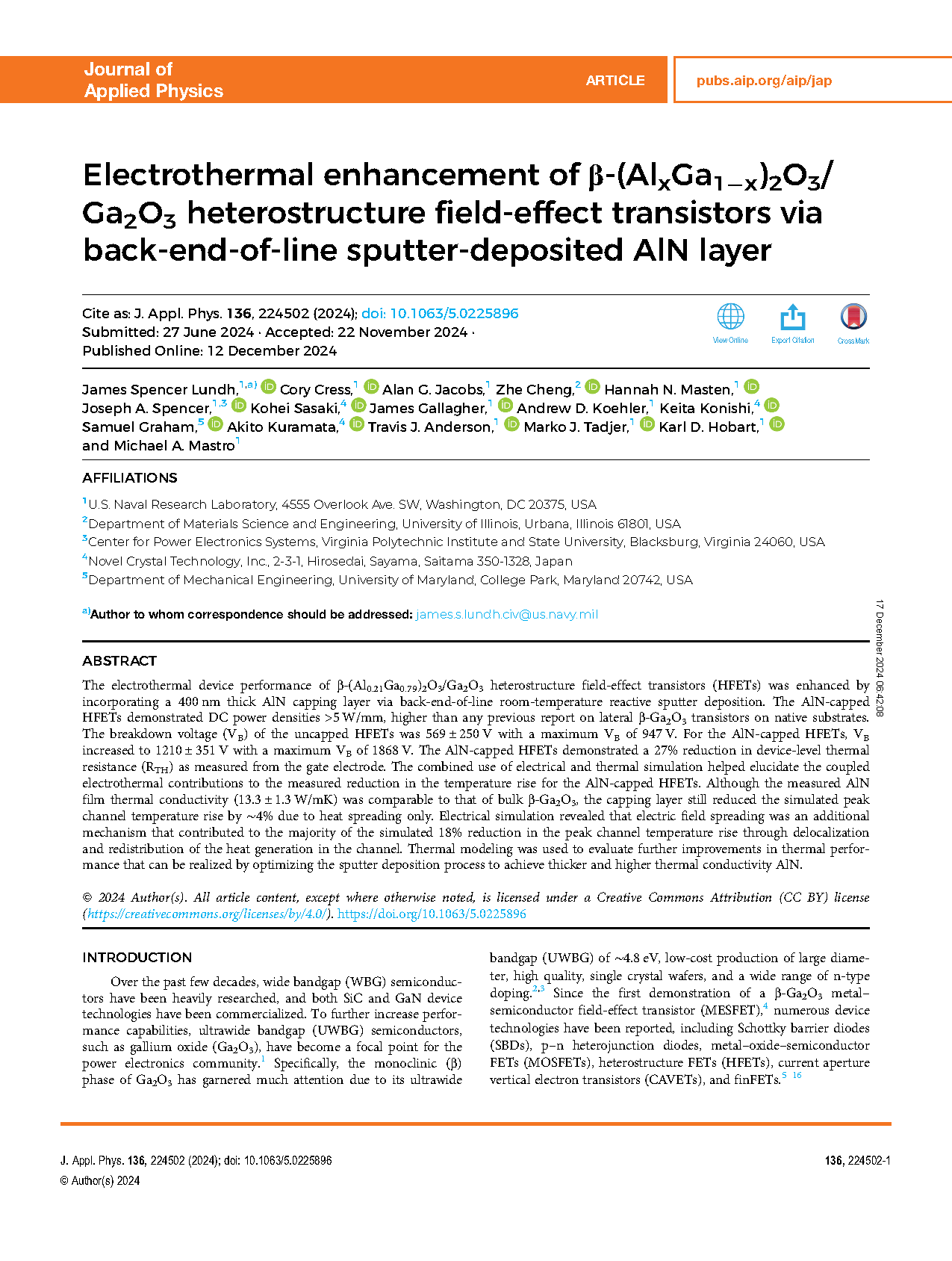
FIG. 1. (a) Cross-sectional device schematic of the β-(Al0.21Ga0.79)2O3/Ga2O3 HFET with the 400 nm sputtered AlN capping layer. (b) AFM image of the 400 nm AlN capping layer in the gate-drain channel region of an HFET. The root mean square (rms) roughness was measured to be 3.12 nm.
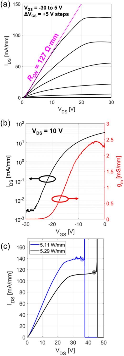
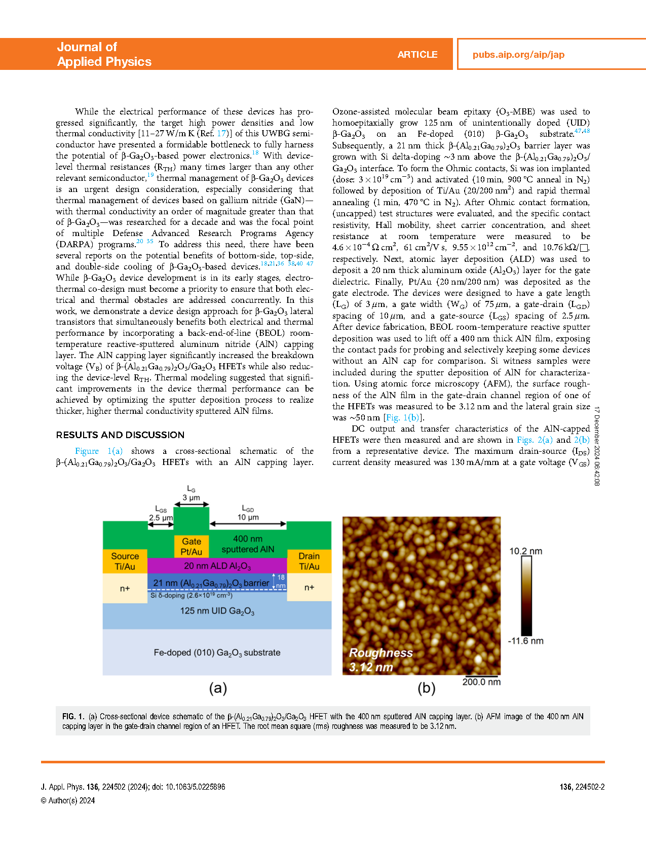
FIG. 2. (a) DC output and (b) DC transfer characteristics of an AlN-capped β-(Al0.21Ga0.79)2O3/Ga2O3 HFET (LG = 3 μm, WG = 75 μm, LGD = LGS = 2.5 μm). (c) IDS–VDS measured at VGS = 0 V for the AlN-capped HFETs showing maximum power density reached (see the legend). The circles indicate the datum from which the power density was extracted.
DOI:
doi.org/10.1063/5.0225896