Paper Sharing
【Domestic Papers】 South China Normal University——Gate-tunable positive and negative photoresponses based on a mixed-dimensional Ga₂O₃/WSe₂ junction field-effect transistor for logic operation
日期:2025-02-13阅读:821
Researchers from the South China Normal University have published a dissertation titled "Gate-tunable positive and negative photoresponses based on a mixed-dimensional Ga2O3/WSe2 junction field-effect transistor for logic operation" in Photonics Research.
Abstract
Realization of positive and negative optical responses in a single device promises construction of multifunctional optoelectronic devices. This work demonstrates a Ga2O3/WSe2 mixed-dimensional heterojunction junction field-effect transistor (JFET) with positive and negative photoresponse regulatory functions by gate voltage. The device achieves a remarkable negative responsivity exceeding 425 mA/W. Additionally, benefiting from Fowler-Nordheim tunneling (FNT) behavior, the mixed-dimensional JFET exhibited an excellent negative response performance with response and decay times of 50.1 ms and 53.9 ms and a high IOFF/ION ratio of 343 at Vds=1 V and Vg=5 V under 635 nm illumination. Additionally, the JFET’s negative photoresponse is sensitive to both gate voltage and light intensity, which can be used to realize NAND logic gate and optical communication functions. These results unveil the promising potential of mixed-dimensional optoelectronic devices for optical communication, and logic device technologies.
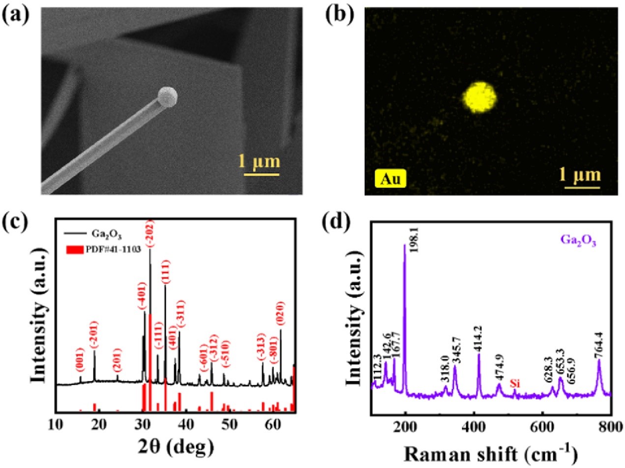
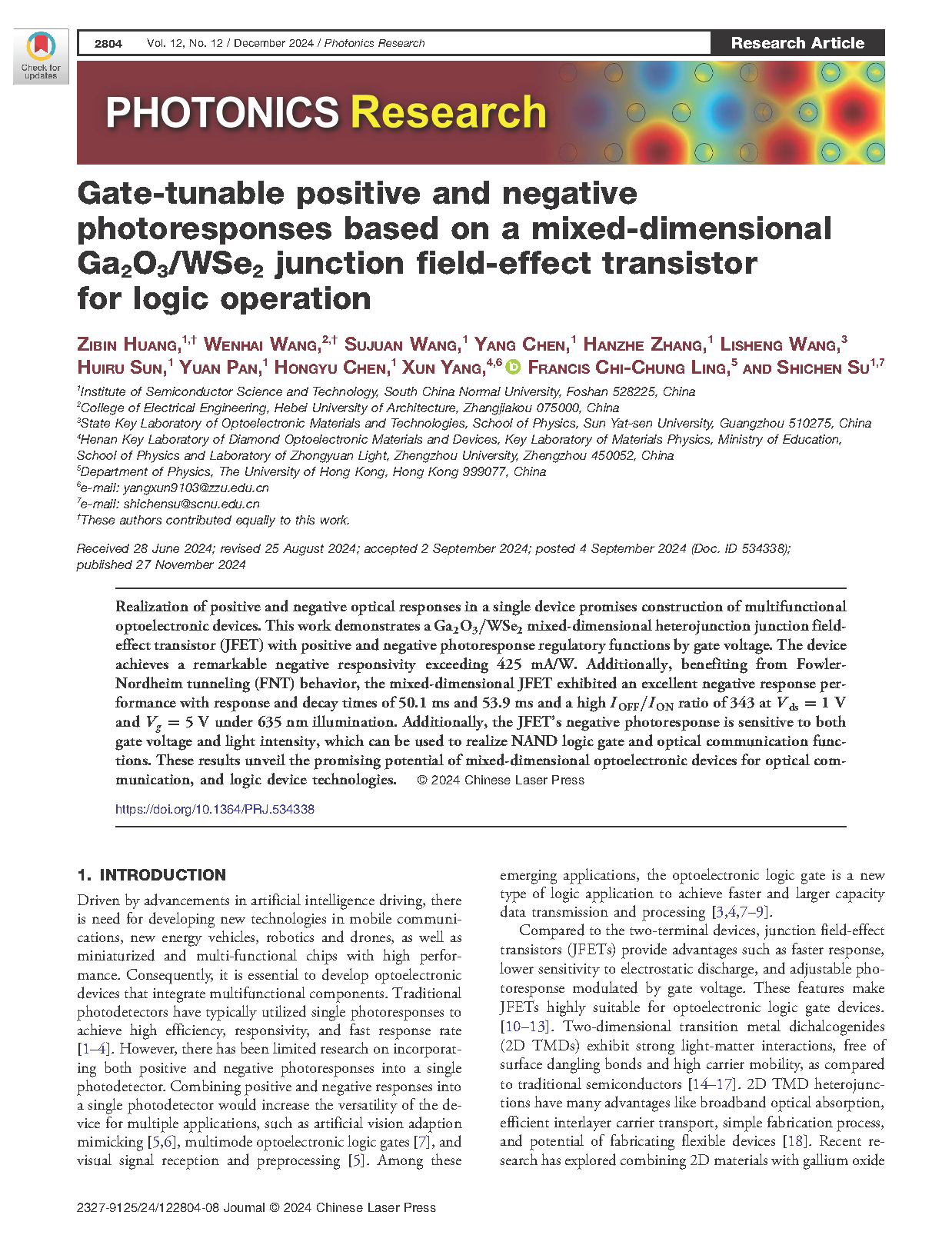
Fig. 1. (a) SEM image of Ga2O3 microwires. (b) EDS mapping image of Au. (c) XRD patterns of β-Ga2O3 microwires grown at 1100°C. (d) Raman spectrum of β-Ga2O3 microwires.
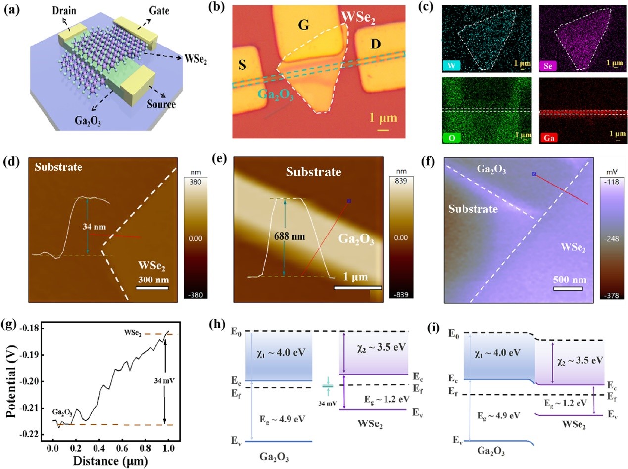
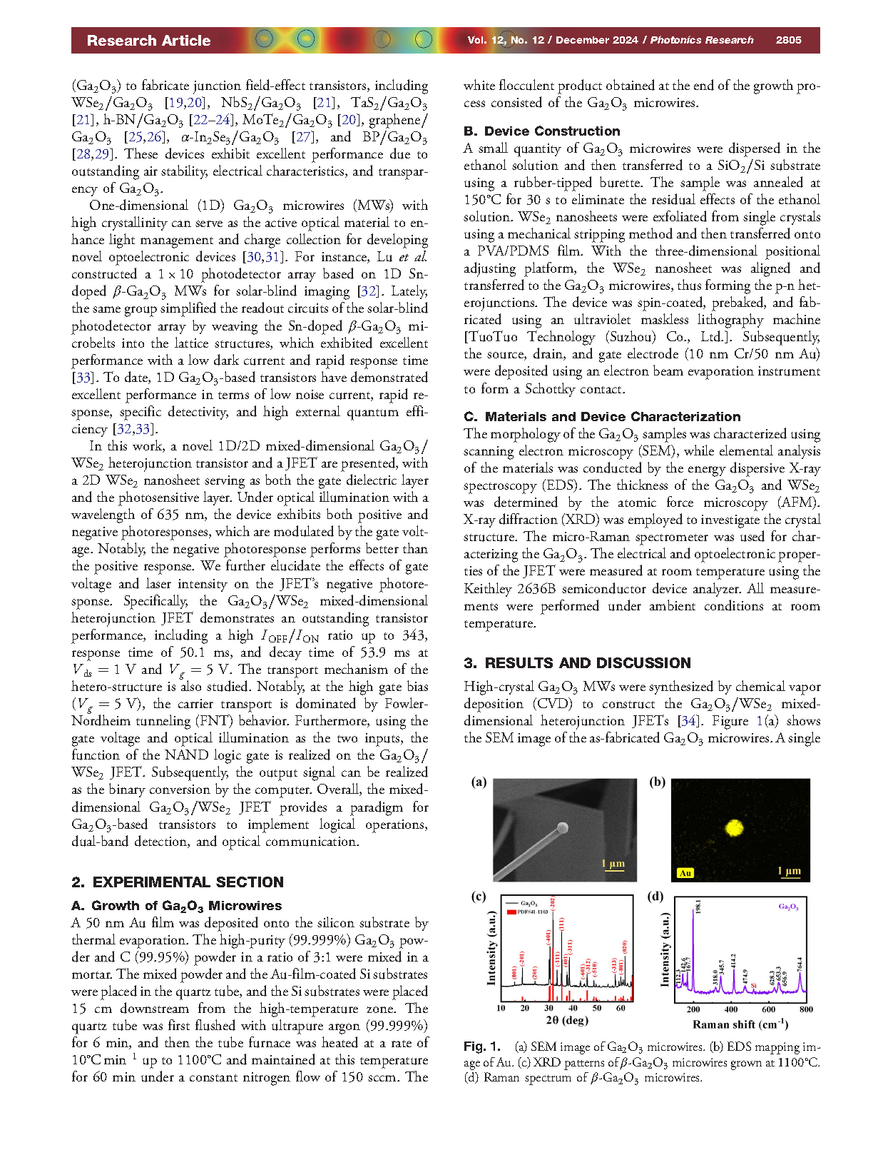
Fig. 2. (a) Schematic illustration of the Ga2O3/WSe2 JFET. (b) Optical microscopy image of the Ga2O3/WSe2 JFET. (c) EDS mapping images of the Ga, O, W, and Se elements. AFM measurement of the thickness of (d) WSe2 and (e) Ga2O3. (f) KPFM image at the Ga2O3/WSe2 interface. (g) SPD plot of the measured Ga2O3/WSe2 interface. Energy band of the Ga2O3/WSe2 heterojunction (h) before and (i) after contact.
DOI:
doi.org/10.1364/PRJ.534338