


Member News
【Member News】Zhang Hongliang's Team of Xiamen University Made New Progress in the Field of Wide Band-Gap Ga₂O₃ Semiconductor
日期:2023-03-14阅读:1334
Recently, Professor Zhang Hongliang from the School of Chemistry and Chemical Engineering of Xiamen University published an academic paper entitled "Deep UV transparent conductive oxide thin films realized through degenerationally dosed wide band-gap gallium oxide" in Cell Reports Physical Science, a sub-journal of material science. This paper reports the Si-doped Ga2O3 wide band-gap semiconductor film with deep ultraviolet transparency and high conductivity, which provides important guidance for the application of wide band-gap Ga2O3 semiconductor in ultraviolet photoelectronic devices, organic semiconductor photoelectronics and high-power electronic devices.

Transparent conductive oxide (TCO) is a unique material, which has both optical transparency and high conductivity -- two seemingly contradictory characteristics. As transparent electrodes, TCO has been widely used in modern photo-electronic fields, including panel displays, solar cells and light-emitting diodes. In recent years, with the rapid development of ultraviolet photo-electronics and organic photo-electronics, a series of new requirements have been put forward for the performance of TCO. For example, AlGaN-based deep ultraviolet lasers and light-emitting diodes require their electrodes to be transparent in the deep ultraviolet region (200 − 300 nm wavelength range). However, at present, the efficiency of such deep ultraviolet LED and laser is quite low (only about 1%), partly due to the lack of deep ultraviolet transparent electrodes. Traditional TCOs, such as Sn-doped In2O3 (ITO), F-doped SnO2 (FTO) and Al-doped ZnO (AZO), have band gaps less than 3.5 eV and are opaque in the deep ultraviolet region. In addition, in organic light-emitting diodes and thin film transistors, the electron affinity of the organic semiconductor layer is 2.5-3.5 eV, and a TCO layer with a work function lower than 3.5 eV is required to add the electrodes so as to improve the efficiency of the organic semiconductor layer. However, the work function of most TCOs is greater than 4.2 eV.
Gallium oxide (Ga2O3) is a new ultra-wide band-gap semiconductor after the third generation of semiconductors such as gallium nitride (GaN) and silicon carbide (SiC). It has outstanding advantages such as wider band gap, higher breakdown field strength and lower cost. It is the preferred material for the new generation of ultraviolet photoelectric devices and ultra-high power devices. Ga2O3 is a semiconductor with ultra-wide band gap (Eg~4.8 eV). It is transparent in the deep ultraviolet spectrum and can be doped with degenerate n-type, which makes Ga2O3 a promising candidate material for deep ultraviolet TCO. However, up to now, the conductivity of n-type doped Ga2O3 is still lower than the minimum value of~103 S/cm required by TCO. The basic photoelectric properties and potential of degenerate doped Ga2O3 thin films as deep ultraviolet TCO have not been fully studied.
Professor Zhang Hongliang of Xiamen University as well as his research team, successfully prepared Si-doped Ga2O3 thin films with ultra-high conductivity and deep ultraviolet transparency by pulsed laser deposition, with conductivity up to 2500 S/cm (Figures 1 and 2). The prepared Si-doped Ga2O3 has a high transmittance of more than 80% from the infrared light region to the deep ultraviolet light region (Fig. 2), which can meet the above requirements of AlGaN-based ultraviolet photo-electronics for transparent electrodes, and has great application prospects. Combined with hard X-ray photo-electron spectroscopy and density functional theory calculation, from the perspective of electronic structure, it is revealed that the key to the high mobility and conductivity of Si-doped Ga2O3 films are the conduction band composed of spatially expanded Ga4s and effective Si doping(Fig. 3). In addition, UV photo-electron spectroscopy shows that the work function value of Si-doped Ga2O3 thin film is very low, 3.26 eV − 3.45 eV, which is far lower than that of traditional TCO (Fig. 4), and can meet the above requirements of organic light-emitting diodes and thin film transistors for the electron injection layer. Further analysis of the energy band structure shows that the low work function of Si-doped Ga2O3 is due to the low electron affinity caused by the conduction band which is formed by Ga4s with high energy. It is worth noting that by introducing the In 5s orbital with lower energy into the conduction band, the work function can be controlled through the alloying of In2O3, which is of great significance for the further commercial application of Si-doped Ga2O3 and its alloys.
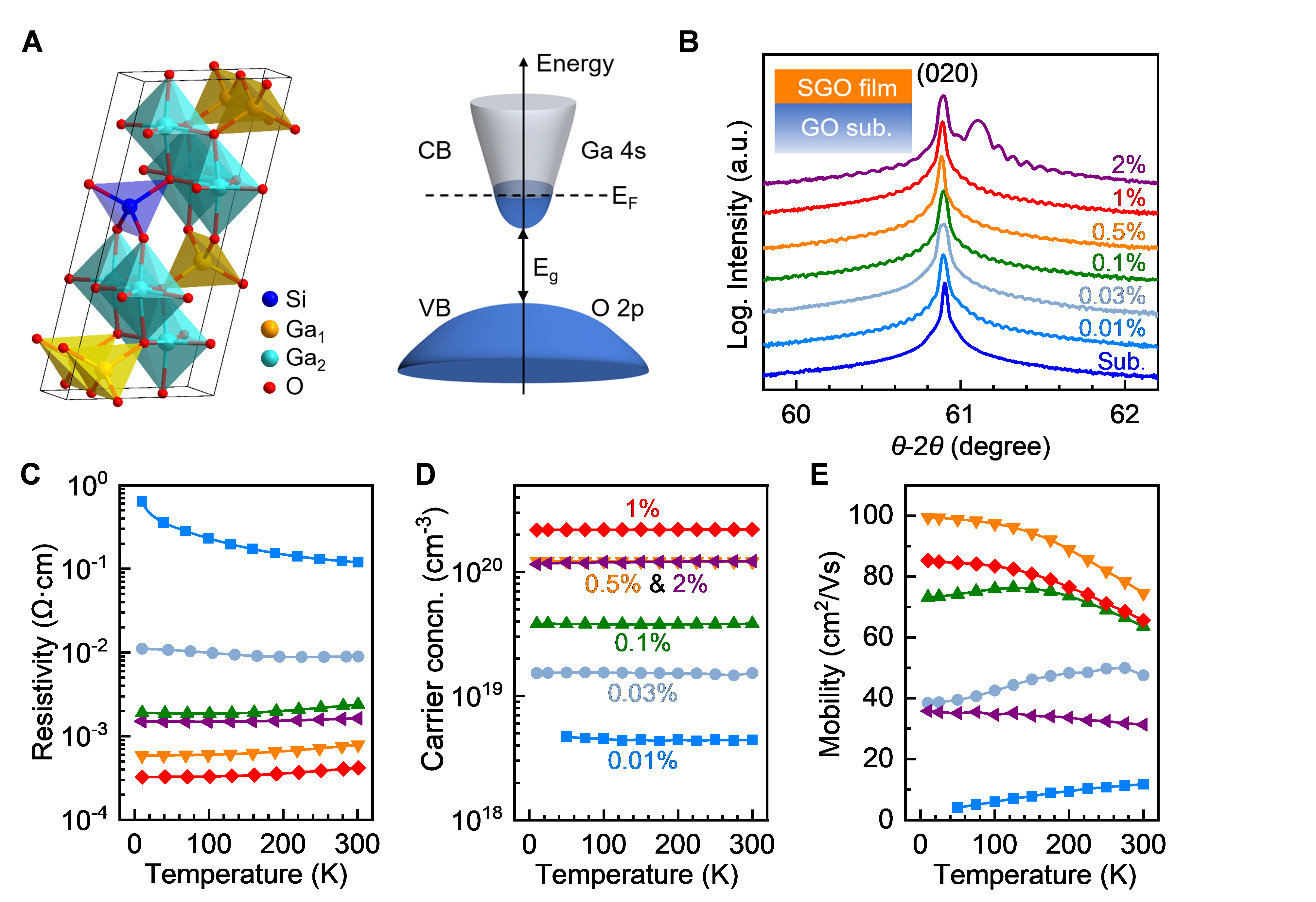
Figure 1. Crystal structure and variable temperature electrical data
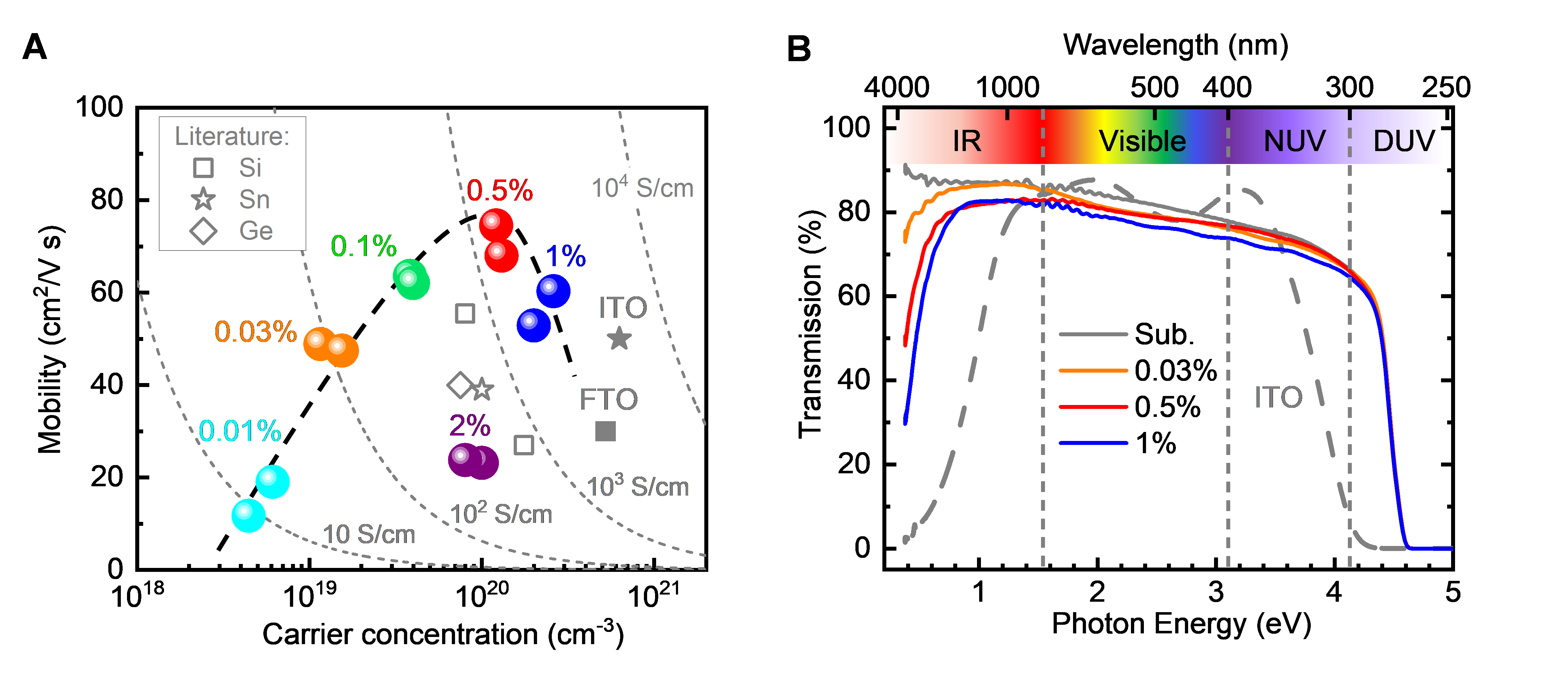
Figure 2. Electrical data and optical transmittance of Si-doped Ga2O3 film

Figure 3. The valence band and conduction band spectra measured by hard X-ray photoelectron spectroscopy and the energy band structure and density of states calculated theoretically
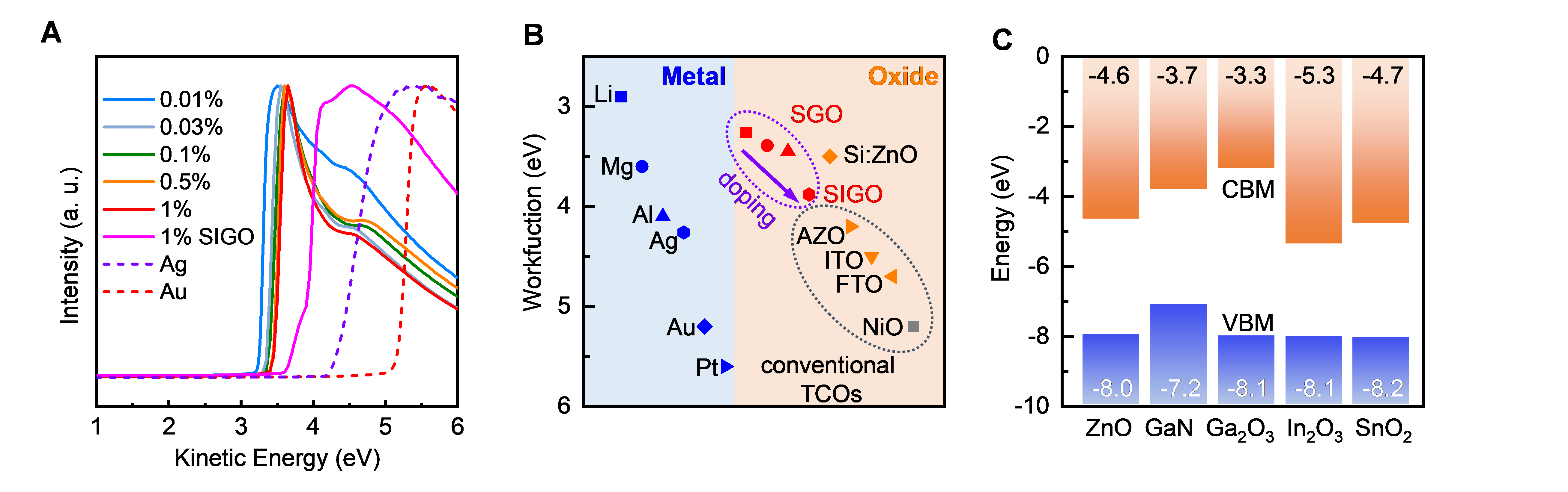
Figure 4. Cut-off edge of secondary electron, work function and energy band position relative to vacuum level, measured by ultraviolet photoelectron spectroscopy
The first author of this paper is Zhang Jiaye, a doctoral student of the Zhang Hongliang Research Team of Xiamen University. The co-correspondents are Zhang Hongliang, Professor Chen Lang of the South University of Science and Technology and Professor David O. Scanlon of the University of London. This work has been supported by the National Natural Science Foundation of China and Shenzhen Science and Technology Research Project.
In recent years, Zhang Hongliang's research team has achieved a series of research results on gallium oxide---a new ultra-wide band gap semiconductor: Ga2O3-based solar-blind ultraviolet photo-detector (Adv. Optical Material., 2022, 10, 2102138.) has been constructed. Through In-doping, the density of states in the valence band has been enhanced, its optical absorption has been improved, and the optical current of the device has been greatly increased. Finally, the switching ratio is more than 108 and the specific detection rate is up to 4.5 × 10¹⁶ Jones. In addition, due to the progress made by Zhang Hongliang's research team in transparent conductive oxides, the research team has got invitations by the editorial departments of APL Material And Adv Mater to write and separately published two summarizes, which entitled "Recent progress on the electronic structure, defect, and doping properties of Ga2O3" (APL Material., 2020, 8, 020906.) and "Wide Bandgap Oxide Semiconductor: from Materials Physics to Optoelectronic Devices" (Adv. Material., 2021, 332006, 230).
Thesis link:https://www.sciencedirect.com/science/article/pii/S2666386422000716?via%3Dihub
