Paper Sharing
【Member Papers】Researchers Led by Academician Yue Hao from the Xidian University——Ga₂O₃ Solar-Blind Deep-Ultraviolet Photodetectors with a Suspended Structure for High Responsivity and High-Speed Applications
日期:2025-02-17阅读:883
Researchers from the Xidian University have published a dissertation titled "Ga2O3 Solar-Blind Deep-Ultraviolet Photodetectors with a Suspended Structure for High Responsivity and High-Speed Applications" in Science Partner Journal.
Abstract
The wide-bandgap semiconductor material Ga2O3 exhibits great potential in solar-blind deep-ultraviolet (DUV) photodetection applications, including none-line-of-sight secure optical communication, fire warning, high-voltage electricity monitoring, and maritime fog dispersion navigation. However, Ga2O3 photodetectors have traditionally faced challenges in achieving both high responsivity and fast response time, limiting their practical application. Herein, the Ga2O3 solar-blind DUV photodetectors with a suspended structure have been constructed for the first time. The photodetector exhibits a high responsivity of 1.51 × 10¹⁰ A/W, a sensitive detectivity of 6.01 × 10¹⁷ Jones, a large external quantum efficiency of 7.53 × 10¹² %, and a fast rise time of 180 ms under 250-nm illumination. Notably, the photodetector achieves both high responsivity and fast response time simultaneously under ultra-weak power intensity excitation of 0.01 μW/cm2. This important improvement is attributed to the reduction of interface defects, improved carrier transport, efficient carrier separation, and enhanced light absorption enabled by the suspended structure. This work provides valuable insights for designing and optimizing high-performance Ga2O3 solar-blind photodetectors.

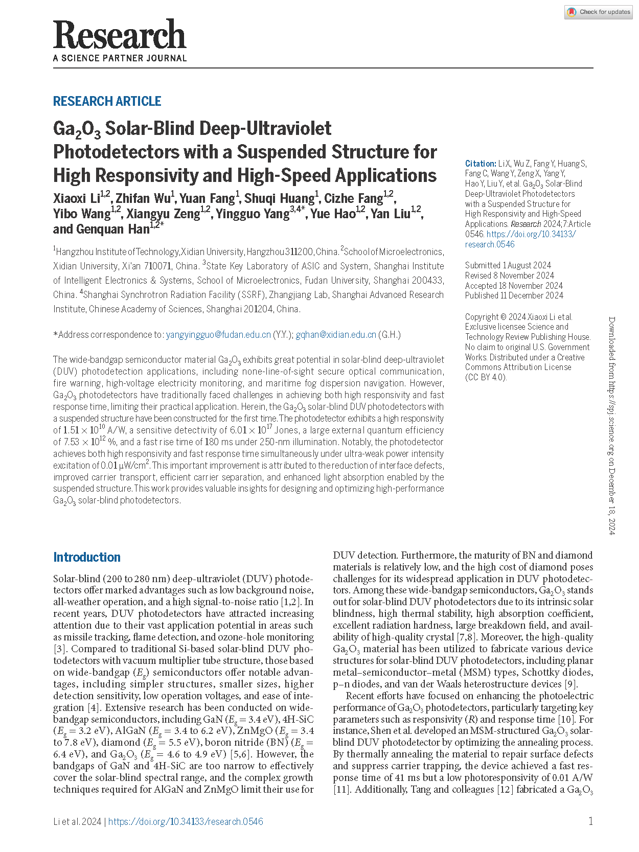
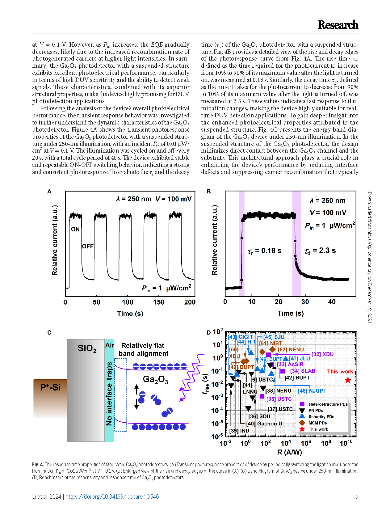
Fig. 1. Characterization of the morphology and height of Ga2O3 devices. (A) Schematic illustration of the Ga2O3 photodetectors with a suspended structure. (B) Depth of the etched trench. Inset: Surface morphology image of the trench. (C) Thickness of the Ga2O3 channel. Inset: Optical microscopic image of the fabricated Ga2O3 photodetector. (D) SEM image of the Ga2O3 device with a suspended structure.
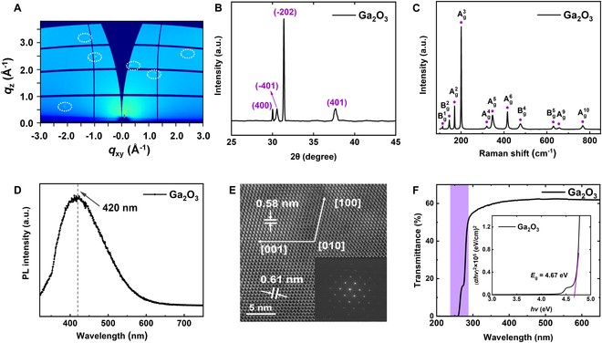
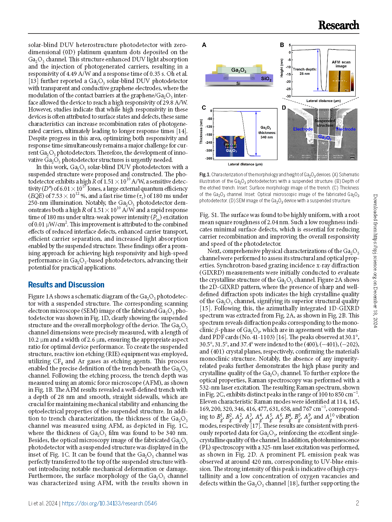
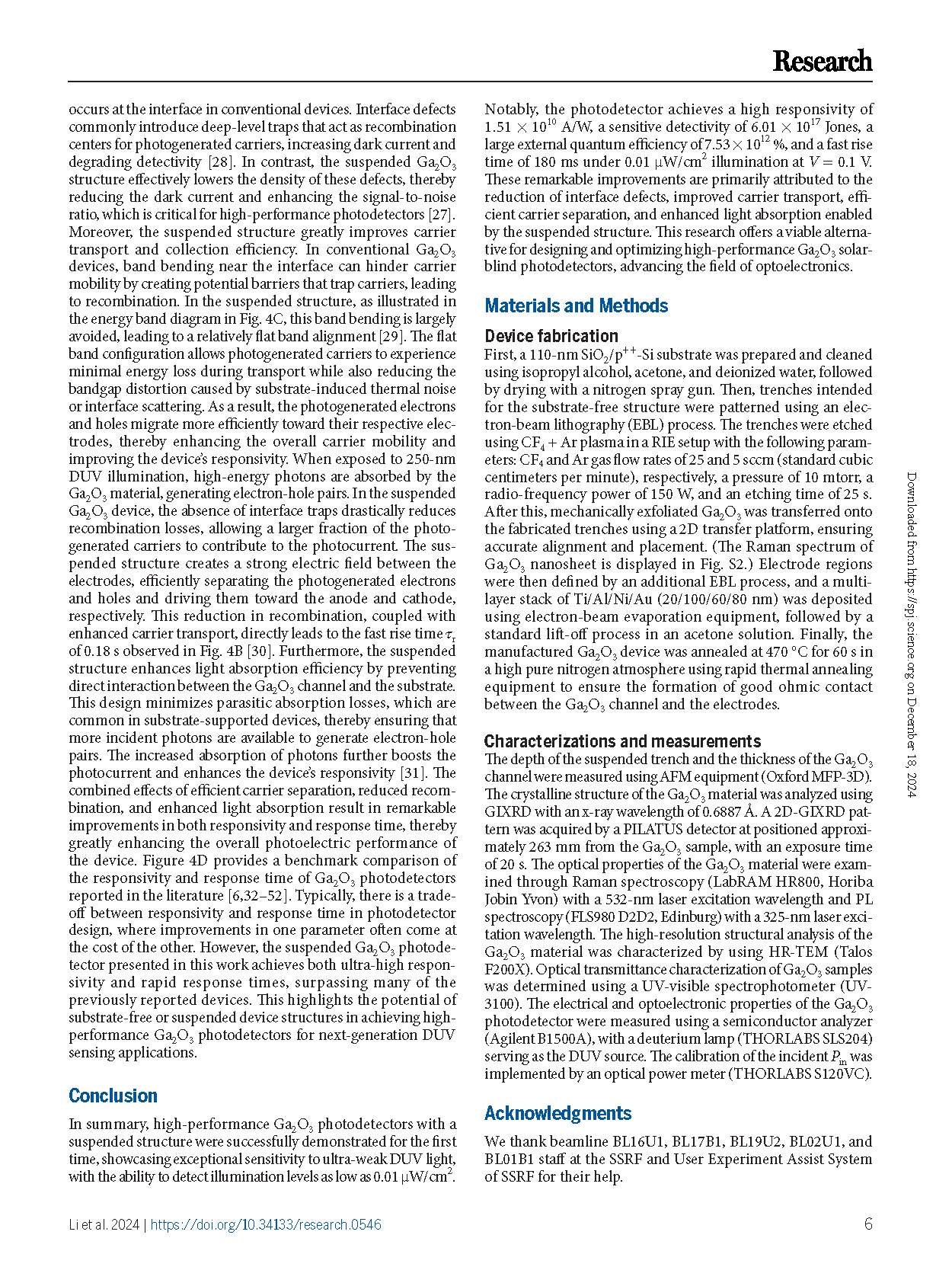
Fig. 2. Material characterizations of Ga2O3 material. (A) 2D-GIXRD pattern of Ga2O3 material. (B) Integrated 1D-GIXRD spectrum of Ga2O3 material. (C) Raman spectrum of Ga2O3 material. (D) PL spectrum of Ga2O3 material. (E) HR-TEM image of Ga2O3 material. Inset: SAED pattern of Ga2O3 material. (F) Transmittance spectrum of Ga2O3 material. The inset displays the curve of (αhν)2 versus hν used to extract the bandgap of Ga2O3.
DOI:
doi.org/10.34133/research.0546