


Paper Sharing
【Domestic Papers】Research on Gallium Oxide Homoepitaxy and Two-Dimensional Step-Flow Growth
日期:2025-02-21阅读:1454
Abstract
How to grow a Gallium Oxide (Ga₂O₃) single crystal film with atomic level flatness by homogeneous epitaxy is the basis for preparing high performance Ga₂O₃ power electronic devices or ultraviolet optoelectronic devices. In this paper, a device-level Ga₂O₃ single crystal film with a thickness of 1.0 μm was prepared (unintentional doping) on a Ga₂O₃ substrate by using metal-organic vapor phase epitaxial (MOVPE) technology to comprehensively control the thermodynamic and kinetic parameters of epitaxial growth. The phase, surface morphology, crystal quality and electrical properties of the film were studied. The film has a single β phase and exhibits the same (100) face preference orientation as the substrate. The surface morphology of the Ga₂O₃ thin film was characterized by AFM and showed a typical step flow morphology with a surface roughness of 0.166 nm and a step height of 0.6 nm (a/2), indicating atomic flatness. Furthermore, the crystal quality of Ga₂O₃ thin films was evaluated by HRXRD twin-crystal rocking curves. The FWHM of the epitaxial films was lower than that of the single crystal substrate, indicating that the quality of Ga₂O₃ thin films epitaxial on the lattice matching substrate was better than that of the substrate. The electrical properties of Ga₂O₃ thin films were analyzed by Hall effect test. The mobility was 92.1 cm2 /(V·s) and the carrier density was 2.65×1016 cm-3. The results of this paper illustrate that it is possible to achieve high and long speed two-dimensional "step flow" growth on a general unintentional chamfer substrate, as long as the transverse diffusion rate in the core kinetic parameters is sufficiently greater than the longitudinal deposition rate by fine regulating the key thermodynamic conditions such as temperature, pressure and Ⅵ/Ⅲ ratio. The (100) planar homogeneous epitaxial single crystal films with excellent crystal quality and electrical properties prepared in this study have important application potential in the manufacture of high performance Ga₂O₃ power electronic devices.
Introduction
In recent years, with the high temperature, high voltage, strong irradiation and other extreme application scenarios, ultra-wide band gap semiconductor materials have been rapidly developed. In particular, Ga₂O₃, which has attracted much attention at present, shows great application potential in the field of high voltage and low loss power devices due to its 4.9eV ultra-wide-band gap, 8 MV/cm high critical breakdown field strength, BFOM of more than 3000 and commercialized large-size single crystal substrate. However, the Ga₂O₃ epitaxy technology is not mature, which restricts its further development in Gallium Oxide power devices. Although metal organic vapor phase epitaxy (MOVPE) technology has been used to fine-control the epitaxy process, and the use of high quality single crystal substrate, the device level Ga₂O₃ epitaxy films have not been successfully realized. Generally, device-level Ga₂O₃ epitaxial films require the formation of single crystal films with atomic-level flatness and low defect density. Due to the existence of non-ideal integer-exponential surfaces on universal substrates (unintentionally chamfer, usually less than 0.5°), two-dimensional "step flow" growth is widely considered to be the ideal way to achieve these high-quality single crystal films and is suitable for the manufacture of high-power electronic devices.
However, the development of Ga₂O₃ materials is still in its early stages, due to the lack of reliable epitaxy equipment, lack of appropriate epitaxy theory, and narrow epitaxy process window constraints, two-dimensional step flow growth is still facing a great challenge. As the main current epitaxy technology for commercial semiconductor electronic devices, MOVPE can accurately regulate the carrier concentration, grow atomically flat single crystal films by In-Situ Growth, and easily achieve a high growth rate of more than 1 μm/h. MOVPE is an ideal choice for preparing a thick drift layer in the core of Ga₂O₃ vertical high withstand voltage power devices. Although the Leibniz Institute for Crystal Growth (IKZ) research team has successfully grows Ga₂O₃ epitaxial films with good step flow surface morphology through MOVPE, two-dimensional step flow growth has not been widely used due to the harsh chamfer substrate processing technology and epitaxial growth rates below 300 nm/h. In addition, there is no mature MOVPE epitaxial equipment available on the market to effectively solve the strong prereaction during the Ga₂O₃ extensional process and the serious oxidative corrosion under high temperature growth conditions, which makes it difficult to achieve the high temperature thermodynamic conditions required for the two-dimensional step flow to grow, that is, can’t promote the deposited atoms to have sufficient lateral diffusion coefficient. Although RF heating alleviates this problem to a certain extent, due to the increasing size of the Ga₂O₃ epitaxial wafer, they still face the problem of poor homogeneity uniformity over a large area. Therefore, only by modifying the existing MOVPE equipment or independently developing a special extensional device for Ga₂O₃, can the conditions for two-dimensional "step flow" ₃ be strictly met.
In the thermodynamic theory of epitaxial growth, two-dimensional growth usually occurs when the interface energy and stress between the substrate and the epitaxial layer are small, which allows the epitaxial layer to easily cover the entire substrate surface. However, the theory does not fully account for the possibility of tridimensional growth in some homogeneous epitaxial systems where the interfacial energies are negligible. The development of epitaxial kinetics theory has made up for this deficiency, emphasizing that the key to achieving two-dimensional "step flow" growth is to ensure that deposited atoms can achieve transverse thermal diffusion on the surface platform of the platform-step-node (TSK) model fast enough until the atoms reach the step or node, thus avoiding new nucleation before the bottom layer is completely covered. For β-Ga₂O₃, the monocline crystal structure of the asymmetric semiconductor material causes significant anisotropy in the C-axis and A-axis directions, which causes the epitaxial growth to change from three-dimensional to two-dimensional in the early stages, becoming a thermodynamic driving force. In addition, the strain energy in the epitaxial layer is the main thermodynamic factor that induces defect and interface roughness (two major modes of lattice stress release). At the same time, the thermal diffusivity and diffusion length of atoms on the surface are the kinetic factors that determine whether the film can heal smoothly and form a flat surface. Therefore, only by synthesizing and fine-regulating many process parameters in the epitaxial growth process, can strict two-dimensional "step flow" growth be achieved, thus effectively reducing the defect density in β-Ga₂O₃ epitaxial film and realizing atomic-level flat surface.
In this study, the theory of epitaxy thermodynamics and kinetics, our team proposes a strategy that synergically considers the conditions of epitaxy thermodynamics and the factors of growth kinetics. By comprehensively regulating key thermodynamic parameters such as temperature, pressure and Ⅵ/Ⅲ ratio, the transverse thermal diffusivity of deposited atoms on the platform can be accurately controlled during the kinetic process, so that it is fully greater than the longitudinal deposition rate of the epitaxial film, so as to achieve a delicate balance between thermal and kinetic, and finally realize the ideal two-dimensional "step flow" growth. To this end, our team innovatively introduced epitaxial growth factor K(thermal diffusivity/epitaxial rate) into Gallium Oxide materials, which effectively characterized the characteristics of the epitaxial system and the evolution of its growth mode. Specifically, the two-dimensional "step flow" growth of the Ga₂O₃ thin films on the unintentionally chamfer A-side β-Ga₂O₃ single crystal substrate was successfully achieved by the self-developed MOVPE equipment for oxide. Under the condition that the epitaxy growth rate of β-Ga₂O₃ single crystal was regulated to 1.0 μm/h with conventional TMGa and O2 as reactants, the prepared thin film exhibited a typical step flow profile with an root mean square roughness of 0.166 nm. It is smoother than the existing polished commercial hydride vapor phase epitaxy (HVPE) wafers. The excellent electrical properties of unintentional doping (UID) epitaxy with high mobility and low background carrier concentration were obtained by Hall test. This research for the development of thickness can be up to 10 microns device level Ga₂O₃ epitaxial wafer provides a possible, for the high pressure, low loss power device development is of great significance.
Experiment
1.1 Experimental Raw Materials and Preparation Methods
This study adopted a custom 3 x 2 inches (1 inch = 2.54 cm) MOVPE equipment, heating system using resistance wire heating, uniform gas model is a vertical coupling interval spray type, to form the uniformity of temperature field, flow field. The MOVPE system is equipped with a laser reflection probe for on-line monitoring of the reflectance of the Ga₂O₃ film deposited on the Al₂O₃ (c) substrate to observe the growth rate and surface roughness of the epitaxial film in real time. Trimethyl Gallium (TMGa) and Oxygen (O₂) are used as reactants, and high purity Argon (Ar) is used as carrier gas. Homogeneous epitaxial substrate was grown by EFG method provided by Hangzhou Fujia Gallium Technology Co., LTD. that is (100) plane Sn doped and Fe doped unintentionally chamfer single-side polished substrate, the dimensions of which were both 10 mm×10.5 mm×0.5 mm. The homogenous substrate was first annealed in 1000 ℃ oxygen atmosphere for 30 min to repair the surface damage, so as to form the atomic-level flat step flow surface topography. Subsequently, the Ga₂O₃ substrate and the sapphire substrate were put into the graphite tray in the MOVPE reaction chamber for epitaxial growth. The growth temperature was 1000 ℃, the growth pressure was 25 mbar (1mbar=100 Pa), and the VI /Ⅲ ratio was 1100. The growth rate was controlled at 1~ 2μm /h.
1.2 Performance Testing and Characterization
The thickness of the heterogeneous epitaxial film was measured using the Filmetrics F20 film thickness meter to approximate the characterization of the homogeneous epitaxial film thickness.
The reflectance curve during epitaxial growth was collected by a laser reflector with a wavelength of 633 nm integrated with the MOVPE system.
The crystal mass of the homoepitaxial layer is evaluated by the full width at half maximum (FWHM) of the twin-crystal rocking curves. The phase analysis of the β-Ga₂O₃ substrate and the homoepitaxial layer and the rocking curve were measured using a Bruker company produced D8 Advance X-ray diffractometer (XRD) using Cu Kα radiation with wavelength λ=0.15406 nm.
The surface root mean square roughness (RMS) of the homoepitaxial layer was measured using Bruker's Dimension Edge atomic force microscope (AFM).
The optical band gap of the epitaxy sample was approximated by a heterogeneous epitaxial wafer on the sapphire substrate, and the absorption coefficient was evaluated using an ultraviolet/visible spectrophotometer of brand Perkin Elmer and model Lambda 1050+.
The electrical performance tests were first performed by electron beam evaporation of Ti/Al electrodes on the surface of the epitaxial sample and then by Van der Pauw method on the Lake Shore 8404 Hall test system.
Results and Discussion
2.1 Phase Analysis of β-Ga₂O₃ Homoepitaxial
The growth rate of MOVPE in homogeneous epitaxy based on the β-Ga₂O₃ (100) face single crystal was 1.0 μm/h and the growth time was 1 h. Figure 1 (a) and (b) shows respectively based on Sn - doped Fe - doped β-Ga₂O₃ homogeneous epitaxial wafer pictures, all show smooth and bright surface morphology, and there was no significant difference before growth of the surface of the substrate, the macroscopic characteristics shows that the epitaxy growth process embodies the powder particles in the process of the typical prereaction conditions were controlled very well. In the prereaction is particularly important in the growth of Ga₂O₃ epitaxy. If not properly controlled, the tiny particles generated in the pre-reaction will form new nucleation points on the substrate surface, which will induce the formation of defect in the epitaxy process, and then destroy the periodic structure of the lattice. In addition, the strong prereaction may also cause the epitaxy rate to be too slow or even unable to grow. If the phenomenon of "atomization" or "rough edge" appears on the surface of the epitaxial wafer, it usually indicates that there are nanoscale particles or large defect inside the crystal, which may also be caused by too strong pre-reaction.
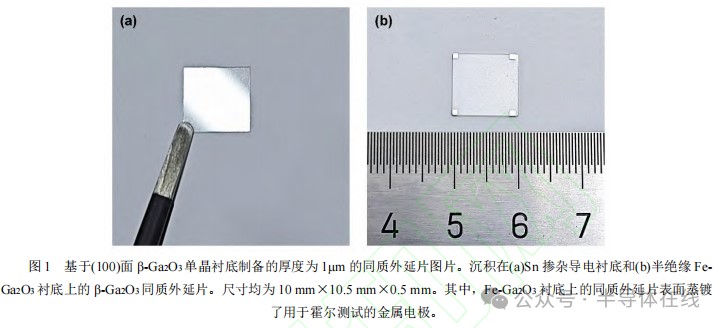
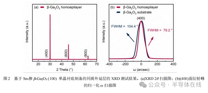
Figure 2(a) shows an XRD 2θ scan of a homogeneous epitaxial film. It can be seen from the figure that the diffraction peaks of the homogeneous epitaxial layer only appear in (400), (600) and (800) three planes (all belong to the 100-plane family of β-Ga₂O₃), and no additional diffraction peaks appear, indicating that the epitaxial film grown is pure phase β-Ga₂O₃ with a single crystal orientation. In order to analyze the crystal quality of the epitaxial layer more comprehensively, the twin-crystal rocking curves of the substrate and epitaxial layer before and after growth were tested by ω scanning tests, and the results were shown in FIG. 2(b). The rocking curves FWHM of substrate and epitaxial layer on (400) plane are 104.4 "and 79.2", respectively. The results show that the crystal quality of homogeneous epitaxial layer is better than that of single crystal substrate. This further indicates that the defect of the substrate does not extend to the epitaxial layer significantly at the initial stage of epitaxial growth, and no additional crystal defect is introduced in the epitaxial process, which effectively improves the crystal quality of the epitaxial layer.
2.2 Optical Properties
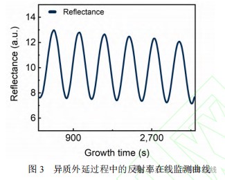
During the epitaxial growth of β-Ga₂O₃, the growth curve of the heteroepitaxial layer can reflect the growth behavior of the homoepitaxial layer to a certain extent. FIG. 3 shows the reflectance curve corresponding to the optimized epitaxy process. During the whole epitaxial growth process, the amplitude of the reflectance curve remained relatively stable, indicating that the roughness of the epitaxial layer did not change significantly, so it can be inferred that the crystal quality of the epitaxial layer did not decrease significantly.
2.3 Surface Morphology Characterization and Epitaxial Growth Pattern Analysis
During the epitaxial growth of β-Ga₂O₃, the ideal homogeneous epitaxial process aims to accurately replicate the symmetry of the substrate lattice, which is manifested by high temperature driving the deposited atoms to rapidly diffuse to the steps or nodes on the T-S-K surface, thus achieving two-dimensional "step flow" growth. However, to achieve the ideal two-dimensional "step flow" growth state requires a lot of process exploration and summary, in order to identify various factors that cause the growth pattern to deviate from the ideal state, and then guide the subsequent process adjustment. In the process of film epitaxial growth, affected by residual stress, growth rate, substrate chamfer angle and other factors, the two-dimensional growth pattern can be further subdivided into two-dimensional "step flow" growth pattern and layer-by-layer growth pattern (also known as two-dimensional Volmer-Weber growth model). And step bunching growth model. From the perspective of epitaxial growth kinetics theory, when the time from reaching the surface of the platform to being adsorbed to the edge of the step is much less than the nucleation time, that is, when the atom diffused on the platform is extremely fast, most of the atoms will be adsorbed to the step, and the epitaxial process shows a two-dimensional "step flow" growth model. When the two time scales are similar, a two-dimensional island is easily formed on the platform. If the lateral growth rate of the islet is fast enough, and the new islet has not yet nucleated above the adjacent step during lateral growth, the epitaxial process still maintains the two-dimensional island growth model, although its surface roughness is higher than that of the two-dimensional "step flow" growth model. If these conditions are not met and the bottom layer is not fully covered, the new islet may nucleate on top of the old islet, resulting in a transformation of the growth model to a three-dimensional island.
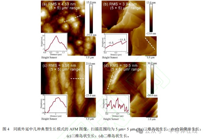
Specifically, the key parameter that determines the type of two-dimensional growth model is closely related to growth factor K(K=D/F), where D is the thermal diffusion coefficient of surface deposition atom, which is directly related to growth temperature. F is the deposition rate of the epitaxial layer. The smaller the K factor is, the easier it is to enter the layer to layer growth mode, and the surface roughness of the film is higher. In the case of large residual stress, excessive K factor leads to the formation of step bunching growth mode. FIG. 4 shows some typical failures in the initial research to regulate the two-dimensional "step flow" growth based on the above theories. The surface roughness of the epitaxial layer is characterized by AFM and RMS values, and the morphology of the film changes under different growth conditions are illustrated.
The typical island morphology in FIG. 4(a) shows that because the epitaxial growth temperature is too low, the thermal diffusion coefficient D is small, and the deposited atoms lack enough energy to complete the lateral migration. Thus, when the bottom layer is not completely covered, new islands form on top of the existing ones and enter the three-dimensional island growth mode. The dashed white lines in the illustration show the dramatic rise and fall in surface height, reflecting the characteristics of this growth pattern. The lamellar structure in Figure 4(b) shows that excessive temperatures cause the step bunching and growth. The excessive temperature increases the K factor, which causes the step to bunching and forms the height fluctuation of several atomic layers. However, the twin-crystal rocking curves FWHM of the epitaxial film did not widen significantly compared with that of the substrate (not shown), indicating that the growth mode did not significantly affect the crystal quality of the epitaxial layer. Although this growth mode helps to relieve residual stress, it is not conducive to achieving atomically flat surfaces. Figure 4(c) reflects the three-dimensional island growth caused by excessive deposition rates, with a significant increase in the FWHM of the XRD half-peak (not shown). This phenomenon is mainly due to the high molar flow rate of reactants, which leads to the failure of timely consumption of reaction raw materials, and when the bottom layer is not covered, new islands are formed on top of the old ones. In this case, in order to achieve two-dimensional "step flow" growth, it is necessary to improve the growth model by reducing the molar flow of reactants or appropriately increasing the growth temperature. FIG. 4(d) shows the two-dimensional island morphology with significant lamellar structure, which may be due to the low VI /Ⅲ ratio in the epitaxy growth process (that is, the relatively insufficient oxygen content) resulting in a small K factor, resulting in two-dimensional island growth.
The above growth modes cause the surface fluctuation and roughness of the Ga₂O₃ epitaxial layer to increase significantly, which is not favorable to the harsh demand of Ga₂O₃ high withstand voltage power devices for flat surfaces. In order to realize the ideal two-dimensional "step flow" growth, it is necessary to optimize the thermodynamic conditions, including temperature, pressure, Ⅵ/Ⅲ ratio, and deposition rate, so as to ensure that the transverse thermal diffusion rate of deposited atoms is significantly higher than the longitudinal deposition rate, so as to achieve the thermal and kinetic balance of the epitaxy growth process.
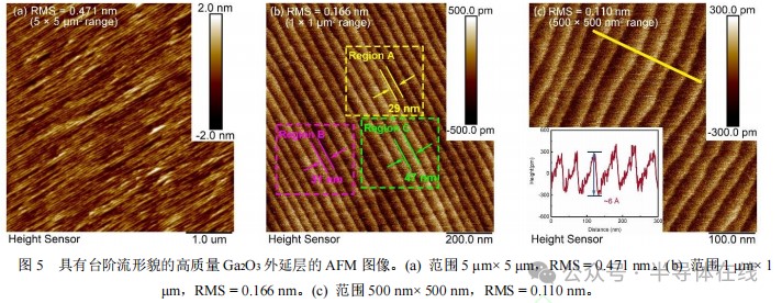
By analyzing and summarizing the failure experience encountered in the process of epitaxy growth, the key parameters affecting epitaxy growth were systematically optimized in this study, including thermodynamic conditions (temperature, pressure, VI /Ⅲ ratio) and kinetic parameters (diffusion coefficient, deposition rate). This optimization ensures that the growth factor K is within the appropriate range, and achieves the accurate balance that the transverse thermal diffusivity D of the deposited atoms is fully greater than the longitudinal deposition rate F of the epitaxial layer. Thus, high-quality homogeneous epitaxial films grown in a two-dimensional "step flow" mode are successfully prepared. The results are shown in FIG. 5. FIG. 5(a) shows an AFM image of a 5 μm×5 μm region on the surface of the homogeneous epitaxial sample. The epitaxial layer surface presents a highly ordered step flow topography, and the RMS value is 0.471 nm. FIG. 5(b) shows another AFM image of a 1μm × 1μm region on the same epitaxial layer, showing a finer surface structure with an RMS value of only 0.166 nm. The surface of the epitaxial layer shows a more regular step morphology. The step widths of regions A, b and C in FIG. 5(b) are 29, 31 and 47 nm, respectively, which may be due to the different width of the substrate step in these regions. The scanning results of the smaller regions on the epitaxial layer are shown in Figure 5(c), with the RMS reduced to 0.110 nm. As can be seen from the profile line illustrated in Figure 5(c), the height of the upper step of the epitaxial layer is about 6 Å, which is close to 1/2 of the lattice constant of the β-Ga₂O₃ a-axis, indicating that the epitaxial layer has an atomic level of flatness.
2.4 Electrical Properties Characterization
Under the same process conditions, the UID epitaxy layer (thickness 1 μm) on Fe-doped semi-insulated β-Ga₂O₃ substrate was prepared and its electrical properties were measured by Van der Pauw method at room temperature. The results show that the carrier concentration of the epitaxial layer is 2.65×1016 cm3, and the electron mobility is 92.1 cm2 /(V·s). It is noteworthy that despite the high crystal quality and perfect step flow morphology of the homogeneous epitaxial layer, its mobility is not as high as expected. Clearly, AFM images and FWHM values alone are not sufficient to fully evaluate the electrical properties of the epitaxial layer. Electron mobility is influenced by a combination of factors such as crystal quality and unintentional doping. Through thermodynamic and kinetic regulation, the crystal quality of the epitaxial layer has been significantly improved, but at present, the impurities Si remaining on the substrate surface due to processing in the epitaxial process, as well as the unintentional doping elements such as Si, C and H in the epitaxial environment have not been strictly controlled, resulting in more impurity scattering centers, thus affecting the carrier mobility. In addition, these unintentionally doped impurities (especially Si) may form donor-type defect, which in turn lead to higher background carrier concentrations. In future work, the team plans to further control the source of impurities (such as precursors) in the epitaxy growth process, or effectively reduce the background carrier concentration by introducing trace acceptor compensation elements. In addition, considering that the content of methyl radicals formed by triethylgallium (TEGa) at high temperatures is relatively small, the study will also consider mixing the appropriate amount of TEGa to reduce the unintentionally doped C content, so as to further optimize the electrical properties of the epitaxial layer.
Conclusion
To sum up, due to the many variables and complex system in MOCVD epitaxy, the existing studies on Ga₂O₃ epitaxy are still scattered and no systematic framework has been formed. In this paper, for the first time, the complexity of Ga₂O₃ epitaxial growth was summarized as a relationship between thermodynamic conditions (temperature, pressure, Ⅵ/Ⅲ ratio) and core kinetics (diffusion rate, deposition rate). To solve this problem, our team innovatively proposed that by precisely regulating key thermodynamic conditions such as temperature, pressure and VI /Ⅲ ratio, the transverse thermal diffusivity in the core kinetics parameters could be fully greater than the longitudinal deposition rate, thus realizing an ideal two-dimensional "step flow" growth model with high growth rate. In addition, this paper combined with specific cases to analyze the improper control of thermodynamic or kinetic parameters led to the epitaxial growth deviated from the ideal model, and in-depth discussion of the possible causes of various non-ideal growth models. Based on this, a high quality β-Ga₂O₃ single crystal film with typical step-flow surface morphology and a roughness of 0.166 nm was prepared successfully. XRD results show that the crystal quality of the film is better than that of the homogeneous substrate. Further Hall effect measurements show that the film has a high mobility of 92.1 cm2 /(V·s) and a low background carrier concentration of 2.65×1018 cm⁻ 3, indicating that it has excellent electrical properties and is expected to be applied to vertical high withstand voltage power devices. Follow-up work will further optimize the epitaxy process to reduce the background carrier concentration and improve key electrical properties such as mobility.
