Paper Sharing
【International Papers】Band alignment characterizations of grafted GaAs/(-201)Ga₂O₃ heterojunction via x-ray photoelectron spectroscopy
日期:2025-02-24阅读:813
Researchers from the Journal of Applied Physics have published a dissertation titled "Band alignment characterizations of grafted GaAs/(-201)Ga2O3 heterojunction via x-ray photoelectron spectroscopy" in Applied Physics Letters.
Abstract
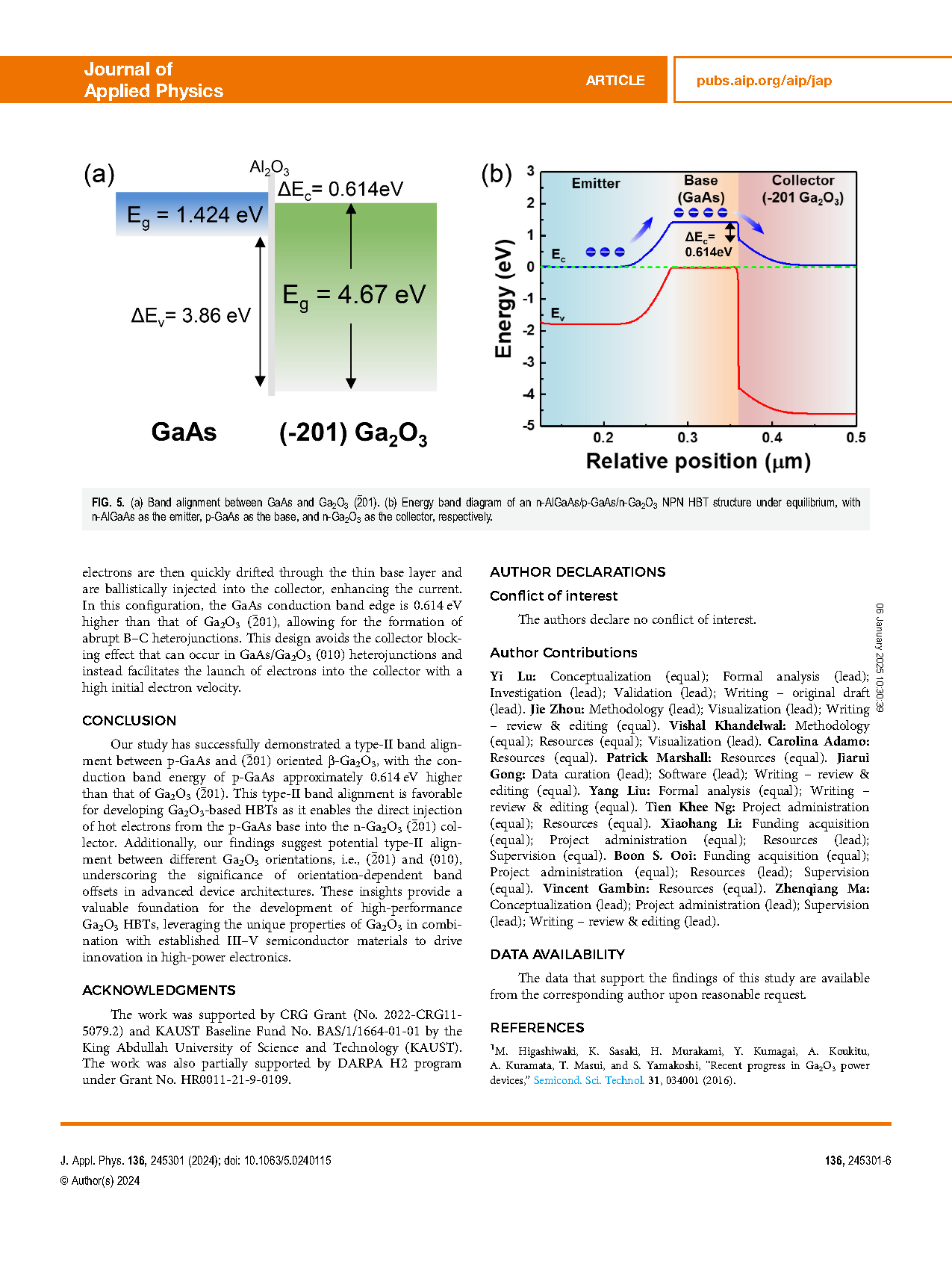
Research on gallium oxide (Ga2O3) has accelerated due to its exceptional properties, including an ultrawide bandgap, native substrate availability, and n-type doping capability. However, significant challenges remain, particularly in achieving effective p-type doping, which hinders the development of Ga2O3-based bipolar devices like heterojunction bipolar transistors (HBTs). To address this, we propose integrating mature III–V materials, specifically n-AlGaAs/p-GaAs as the emitter (E) and base (B) layers, with n-Ga2O3 as the collector (C) to form III–V/Ga2O3 n–p–n HBT. This hetero-material integration could be achieved using advanced semiconductor grafting techniques that could create arbitrary lattice-mismatched heterojunctions by introducing an ultrathin dielectric interfacial layer. This study focused on revealing the band alignment at the base–collector (B–C) junction using a n-Ga2O3 (-201) orientated substrate combined with p-GaAs for potential HBT applications. We discovered a type-II band alignment between p-GaAs and Ga2O3 (-201), with the p-GaAs conduction band approximately 0.614 eV higher than that of Ga2O3 (-201). This staggered alignment allows for direct and efficient electron transport from the p-GaAs base to the n-Ga2O3 collector, avoiding the electron blocking issues present in p-GaAs/Ga2O3 (010) heterojunctions. Additionally, our study suggests the potentially existing type-II alignment between the (-201) and (010) Ga2O3 interfaces, highlighting the orientation-dependent band offsets. These findings are pivotal for developing high-performance Ga2O3-based HBTs, leveraging the strengths of Ga2O3 and well-established semiconductor materials to drive advancements in high-power electronics.
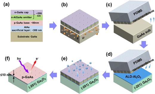
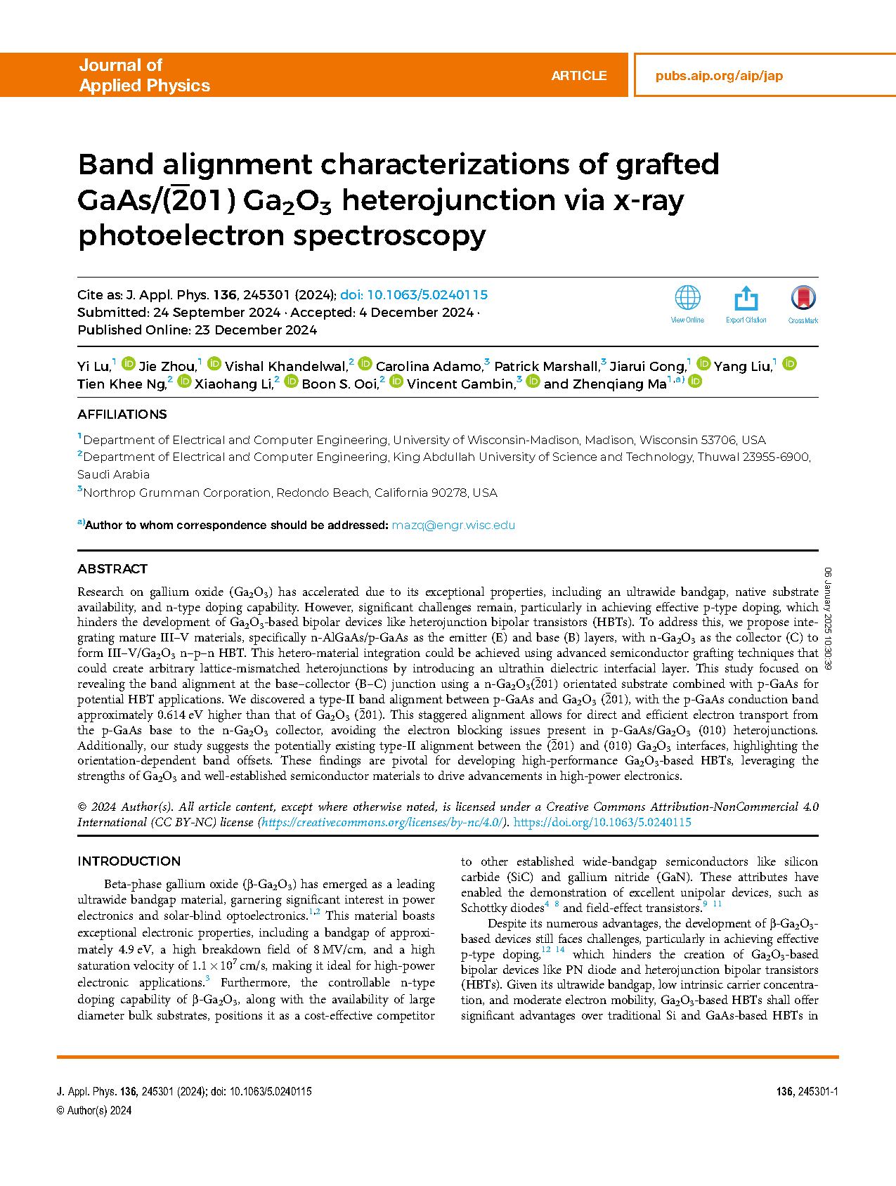
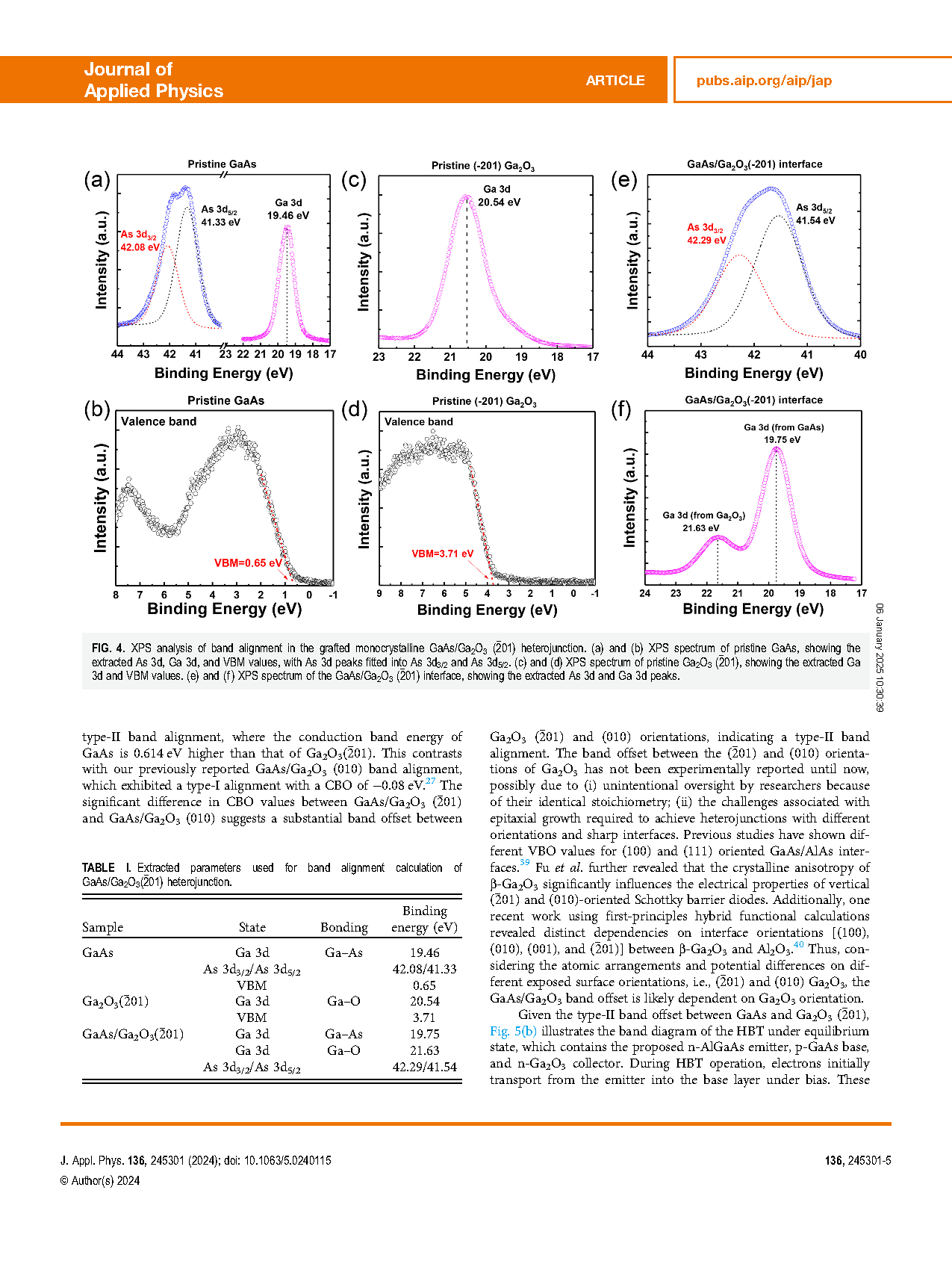
FIG. 1. Fabrication process of the p-GaAs/Ga2O3 (-201) heterojunction. (a) Schematic illustration of the initial n-AlGaAs (emitter) and p-GaAs (base) heterojunction structure. (b) Undercutting the AlAs sacrificial layer at the bottom using the HF solution. (c) Lifting the released NM from the host GaAs substrate using a PDMS stamp, followed by residue cleaning. (d) Transferring the released NM to the Ga2O3 substrate pre-coated with five cycles of ALD-Al2O3, followed by RTA at 350 °C for 5 min. (e) Reducing the NM thickness to ≤10 nm through controlled dry etching. (f) The finalized grafted monocrystalline GaAs/Ga2O3 (-201) heterostructure ready for XPS characterization.
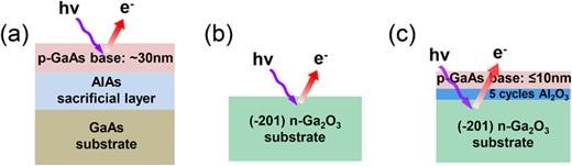
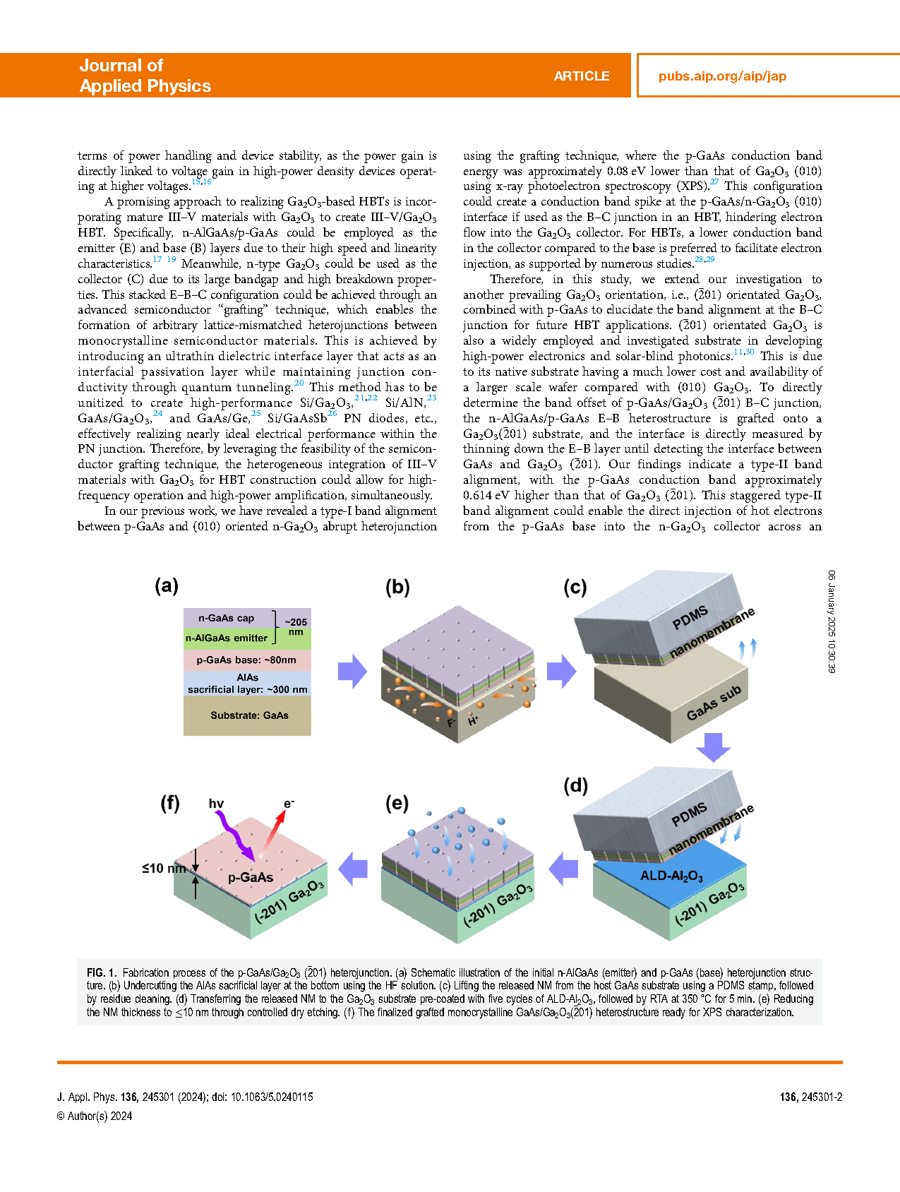
FIG. 2. Schematics of the three investigated samples: (a) pristine p-GaAs, (b) pristine Ga2O3 (-201) substrate, (c) grafted p-GaAs/Ga2O3 (-201) interface.
DOI:
doi.org/10.1063/5.0240115